
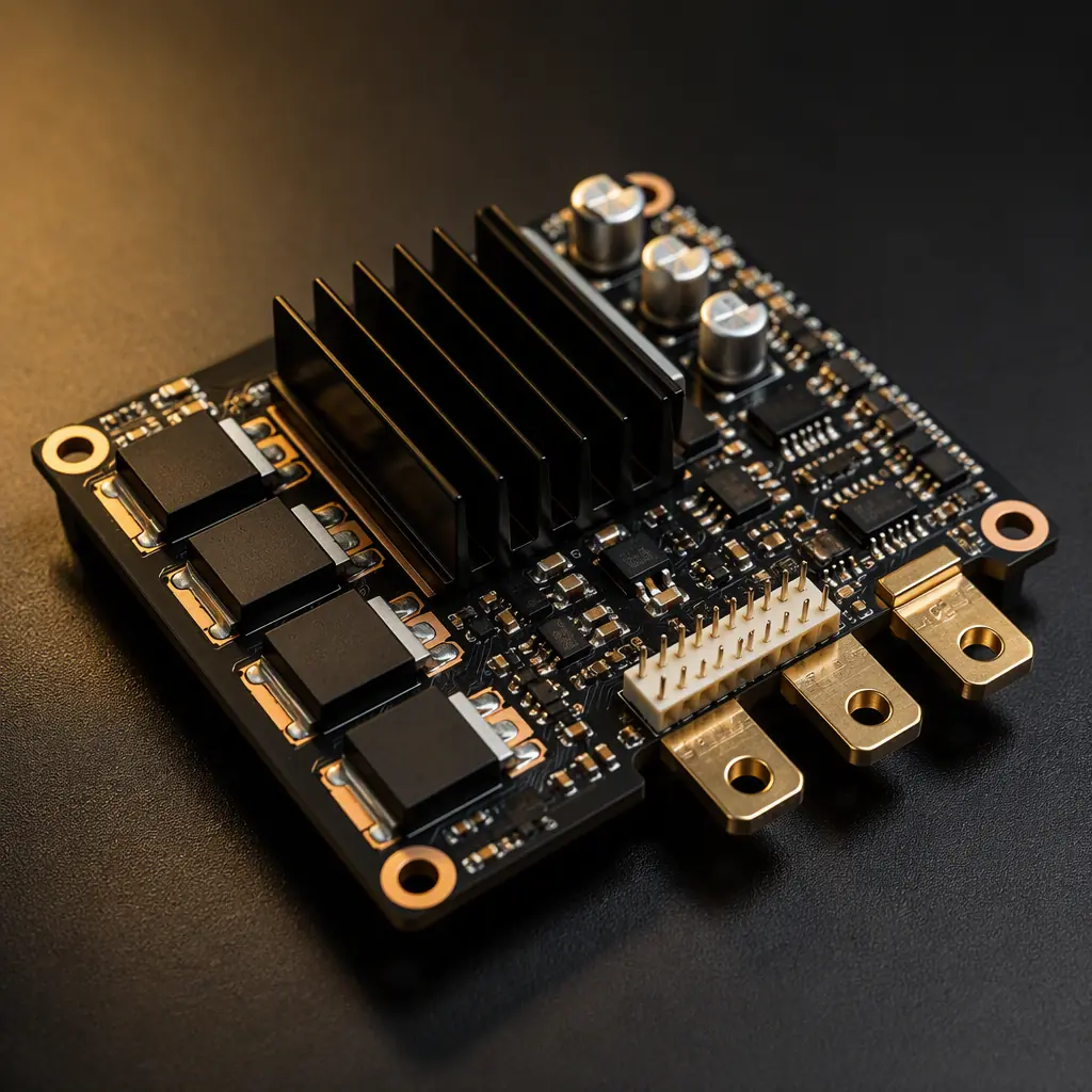
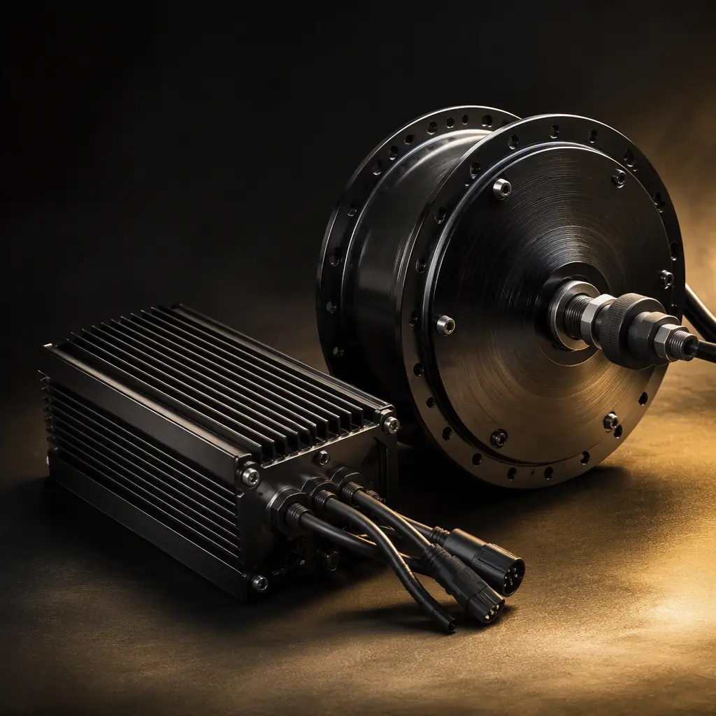
Every e-bike, drone, power tool, robot and appliance that moves is driven by a brushless DC (BLDC) motor. And every one of those motors is driven by a controller board that combines a high-current 3-phase inverter, gate drivers, current sensing, and a microcontroller on one PCB. It is a hostile electrical environment: phase currents of 20–60 A are chopped at 15–30 kHz while the same board tries to measure signals in the microvolt range and keep a 3.3 V MCU alive.
Huaxing PCBA builds motor controller boards for e-bike, micromobility, power tool, robotics and appliance customers, up to 32 layers with 3/3 mil routing, 2–6 oz copper options, and functional test rigs that spin real motors before shipment. This guide covers the six layout disciplines that separate a controller that lasts years from one that fails in the field: the inverter power stage, gate drive, current sensing, commutation feedback, thermal management, and EMC.
Why BLDC Controllers Are a Different PCB Category
A BLDC controller is a switching power converter and a precision analog instrument in the same enclosure. The commutation circuit turns each motor phase on and off six times per electrical revolution, pushing current through the motor winding inductance and back. That switching creates three things every other PCB only deals with one at a time: high di/dt ground noise, high temperature rise, and radiated EMI that couples straight into the control electronics.
Commutation Means the Ground Plane Is Never Quiet
Every PWM edge dumps current into the ground and power planes. If the MCU and the gate drivers share a noisy return path, the controller will misfire. The classic symptom is random commutation glitches at high throttle that disappear when you probe the board. The layout answer is a clean partition between the power half and the logic half, connected at exactly one star point.
The Board Is Also the Heatsink Interface
A 48 V / 25 A controller dissipates 5–15 W in the MOSFETs alone. The PCB copper is part of the thermal path. Which is why motor controller boards so often use 2–4 oz copper and arrays of thermal vias under the power devices. Our copper weight guide covers the specification side; the layout side is covered below.
It Must Survive the Motor, Not Just the Lab
Motors are inductive loads with brushes of electromagnetic energy: back-EMF spikes, cable inductance, and stall conditions. The board has to absorb regenerative energy, clamp voltage transients, and keep running through vibration. That is why controller reliability is mostly a layout and manufacturing-quality problem, not a component-selection problem.
Key Takeaway: Think of the controller as three circuits, power, analog, and digital, that share one board. The layout's job is to keep their ground returns, noise, and thermal paths from destroying each other.
Power Stage Layout: The 3-Phase Inverter Bridge
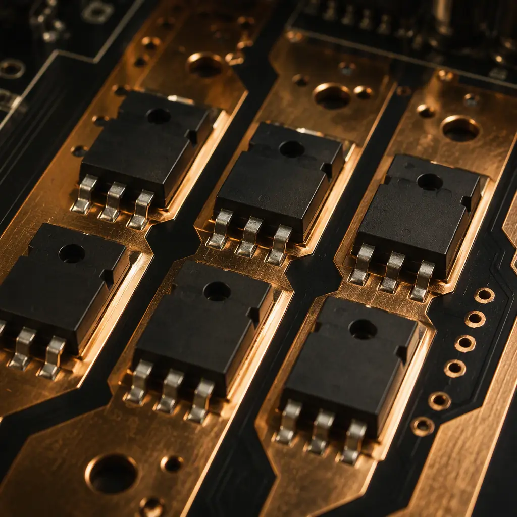
The heart of the controller is the inverter: six MOSFETs arranged as three half-bridges, one per motor phase. The single most important layout rule is to minimize the commutation loop. The path the current takes from the bulk capacitor, through the high-side FET, the phase output, the low-side FET, and back to the capacitor. This loop is the antenna that radiates EMI and the source of the voltage spikes that kill FETs.
Shrink the High-Side/Low-Side Commutation Loop to a Few Square Millimeters
Place each high-side FET directly above its low-side FET (or use a half-bridge module) so the phase node is a short copper island between them, and put the bulk + ceramic capacitor bank within 10–15 mm of the FETs. The parasitic inductance of the loop should be under 10 nH; every extra nanohenry adds di/dt voltage spikes on top of the bus. For 30 A controllers, use 2 oz copper on the power layer and keep the high-current traces at least 3–4 mm wide per 10 A.
Split the Bus Capacitance: Bulk for Energy, Ceramic for Switching
Electrolytic or film capacitors store the energy (typically 470–2200 µF for e-bike controllers); ceramic capacitors (0.1–1 µF, multiple in parallel) handle the high-frequency switching current right at the FETs. The ceramics must sit closer to the drain-source path than the bulk caps. Their job is to supply current during the tens of nanoseconds of each switching edge.
Match the FET Voltage Class to the Application, Then Add Margin
Typical selections: 36–48 V e-bike systems use 75–100 V FETs; 4S–6S drones use 40–60 V; 20 V power tools use 60 V. The margin absorbs switching spikes and regenerative braking overshoot. Our EV traction inverter guide shows the same discipline scaled up to 800 V silicon carbide.
| Application | Bus Voltage | Phase Current | FET Voltage Class | Copper Weight |
|---|---|---|---|---|
| Drone ESC (4S-6S) | 14.8–22.2 V | 20–40 A peak | 40–60 V | 2 oz |
| E-bike / scooter | 36–48 V | 15–30 A | 75–100 V | 2–3 oz |
| Power tool | 18–20 V | 30–60 A peak | 60 V | 3–4 oz |
| Robot / industrial | 24–48 V | 10–40 A | 75–100 V | 2–4 oz |
Gate Driver Placement: Distance Is the Enemy
The gate driver converts the MCU's 3.3 V logic into the 10–15 V, high-current pulses that actually switch the MOSFET gates. The layout relationship between driver and FET is as important as the components themselves.
Keep the Driver Within 10 mm of Its MOSFETs
Gate drive traces carry fast edges into a capacitive load (the FET's gate, typically 5–30 nC). Long traces add inductance that causes ringing on the gate waveform, which translates directly into switching loss and EMI. Route the gate signal as a short, wide trace (0.5 mm+) with the gate resistor placed right at the FET gate pin, the resistor damps the ringing and controls the slew rate.
Use the Kelvin Source Connection for High-Current FETs
In a TO-220 or DFN power FET, the source pin carries both the main current and the gate return. The voltage drop across that shared inductance appears on the gate drive and can cause parasitic turn-on. A Kelvin source connection gives the driver its own dedicated return path to the source pad, decoupling the drive loop from the power loop. If the FET package has a separate source sense pin, use it.
Plan the Bootstrap Supply on the Layout
High-side drivers need a bootstrap capacitor that floats with the phase node. Place the bootstrap cap and its diode within 5 mm of the driver's high-side pins, with the cap's ground return going straight to the phase node, not through the logic ground. A poorly placed bootstrap cap is one of the most common causes of high-side drive failure at high duty cycles.
Current Sensing: Shunt, Kelvin Routing & the Amplifier
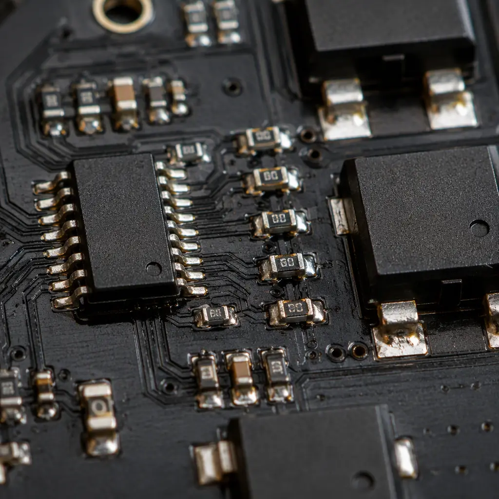
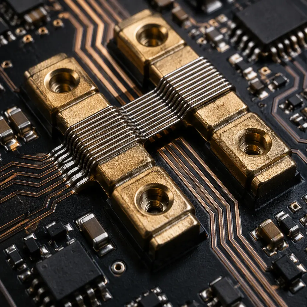
The controller must know the phase current for torque control, overcurrent protection, and commutation timing. The most common method is a low-side shunt resistor measured differentially by an amplifier. The measurement is microvolt-level, a 2 mΩ shunt at 30 A drops only 60 mV, sitting inches away from 30 A of switching current. Layout is everything.
Use 4-Wire Kelvin Routing to the Shunt
Route the sense traces directly from the shunt's own pads, one pair for the current path, one pair for the sense path, never tap the sense lines off the power trace. The sense traces should be thin, short, equal-length, and run close together (a twisted pair in PCB form) to reject common-mode noise. Route them on an inner layer if possible, away from the phase nodes.
Put the Amplifier Next to the Shunt, Filter Right at the Amplifier
The differential amplifier (or the MCU's internal PGA) should sit within 5–10 mm of the shunt. Add a small RC filter (e.g. 100 Ω / 1 nF) directly at the amplifier inputs to knock down the switching spikes before they reach the converter. The filter corner should be well above the PWM frequency but below the noise spectrum: typically 100 kHz–1 MHz.
Choose Shunt Value and Power Rating Together
A 1–5 mΩ alloy shunt is typical. The tradeoff: lower value = less power loss but smaller signal; higher value = better resolution but more heat and voltage drop. At 30 A continuous through 2 mΩ, the shunt dissipates 1.8 W. It needs its own copper area and a 2–3 W rating, not a 0.25 W resistor. For three-phase sensing, use three shunts (one per low-side FET) or a single DC-link shunt depending on the control algorithm.
| Sensing Method | Signal Level | Pros | Layout Cost |
|---|---|---|---|
| Low-side shunt (per phase) | 30–75 mV at rated current | Cheap, accurate, standard | Kelvin routing required |
| DC-link / bus shunt | Same, one shunt | One sense point | Cannot see phase current directly |
| Hall / current sensor IC | Analog out, isolated | No power loss, isolated | Costlier, still needs layout care |
| Motor phase resistance (sensorless) | Computed | No hardware | Needs clean ADC reference |
Commutation Feedback: Hall Sensors, Encoders & Back-EMF
The controller needs rotor position. Hall sensors mounted on the PCB (or in the motor) give absolute position for commutation; encoders add precision; sensorless designs measure back-EMF through the phase nodes. Each approach has layout implications.
Route Hall Signals as Short, Filtered Triplets
Hall sensor outputs are low-level signals riding on a noisy motor environment. Keep the three hall traces short and parallel, add 0.1 µF bypass caps at each sensor, and terminate them with pull-ups near the MCU. If the sensors are in the motor rather than on the controller, the connector carries them, use twisted pairs or a shielded cable and add RC filtering at the MCU pins.
Give the ADC a Clean Reference for Back-EMF Sensing
Sensorless controllers measure the motor's back-EMF through resistor dividers connected to the phase nodes. Which are also the noisiest points on the board. The divider network must be close to the MCU, well-filtered, and referenced to the analog ground, not the power ground. This is where a mixed-signal layout discipline pays off; our mixed-signal design guide covers the partitioning rules in detail.
Separate the MCU Power Domain From the Gate Drive Supply
The MCU should run from its own LDO with a dedicated ground return to the star point. The 12–15 V gate drive rail and the 3.3 V logic rail should never share a regulator or a long common trace. Switching current from the driver supply will modulate the logic rail and cause brownouts exactly when the motor is drawing maximum current.
Thermal Design for Continuous Motor Current
Heat is the number one field-failure driver in motor controllers. The MOSFETs dissipate most of it, and the PCB is part of the cooling path between the die and the heatsink or enclosure.
Use 2–4 oz Copper and Flood the FET Footprints
Copper weight directly increases the thermal spreading area of the board. Under each power FET, flood the pad with as much copper as the design allows and connect it to a large pour on the bottom layer with thermal vias. Our thermal management guide explains the via-array math; a typical rule of thumb is a 3×3 to 5×5 array of 0.3 mm vias under each FET tab.
Design the Thermal Path From the Start, Not as a Fix
Decide early whether the FETs cool through a heatsink on the bottom of the board (via a thermal pad), through a metal-core substrate, or through the enclosure. Each changes the stackup, the solder mask openings (vias filled or tented), and the assembly process. A controller redesigned for heat late in the project costs more than one planned for it.
Protect Against Thermal Runaway With Layout-Level Sensing
Place an NTC thermistor near the FET bank (not near a capacitor or the MCU) and route its traces to the ADC with the same care as the current sense. Firmware can then derate current as temperature climbs instead of letting the board cook. A well-placed NTC on a 2 oz board reads the FET temperature within 5–10 °C, close enough to protect the hardware.
EMC: The Motor Cable Is an Antenna
The phase wires between controller and motor are the best antennas on the product, they carry 20 kHz PWM edges into an inductive load. Every controller design fights conducted and radiated emissions, and most of the fight is won on the PCB.
Add RC Snubbers Across Each Half-Bridge
A snubber (e.g. 10 Ω / 1–10 nF) across each FET pair damps the voltage ringing at the phase node, cutting both the spike stress on the FETs and the radiated emissions. The snubber components belong physically between the FETs, not on the other side of the board. Our EMC compliance guide covers the full emissions-control toolkit.
Filter the Motor Outputs and the Power Input
Add a common-mode choke and Y-capacitors at the battery input, and ferrite beads or a small LC filter on the phase outputs where the cable connects. The board's connector footprint should make room for these, a controller with no input filter almost always fails CE/FCC conducted emissions testing on the first attempt.
Keep the MCU and Its Crystal Far From the Phase Nodes
The switching node voltage swings the full bus voltage at every PWM edge; a crystal or a sensitive analog trace passing near it will pick up that energy. Route the phase output traces on the opposite side of the board from the MCU, and keep a ground pour between the power section and the logic section. For high-power controllers, consider a slot or moat in the ground plane to force the return currents onto the intended path.
Manufacturing Requirements for Motor Controllers
Motor controller boards push manufacturing capability harder than most PCBs: thick copper, high layer counts, fine-pitch BGA MCUs, and the requirement that every unit actually drive a motor before it ships.
Heavy Copper Changes the Fabrication Rules
At 3–4 oz copper, minimum trace/space rules loosen (typically 5/5 mil or wider), and the etching process needs to be validated for the thicker foil. Impedance control on mixed 1 oz signal layers and 3 oz power layers requires careful stackup planning. Specify the copper weight per layer in your fabrication notes, not just "2 oz board."
Plan for X-Ray and ICT/Flying Probe Coverage
Controllers with BGA MCUs need X-ray inspection of the BGA joints; high-current solder joints benefit from AOI plus X-ray spot checks. For production volume, the board should include test points for ICT or flying probe coverage, see our test method comparison . Plus a connector footprint for the motor test rig.
Require a Real-Motor Functional Test, Not Just Power-On
A controller can pass every electrical test and still fail in the field because of a marginal gate drive or a noise-sensitive sense path. The most valuable test is a motor spin test: load the firmware, spin a real (or dynamometer) motor through the full speed range, and verify commutation, current limiting, and thermal behavior. Huaxing's functional test service supports exactly this. Boards are tested with the actual load profile before packing.
Key Takeaway: The manufacturing file set matters as much as the schematic: layer-by-layer copper weight, thermal via specifications, test point placement for ICT, and a motor-load functional test procedure all belong in the purchase order, not improvised at first production.
Summary: The Six Disciplines of a Controller That Survives
A reliable BLDC controller comes from six layout disciplines applied together: (1) a tightly looped inverter power stage with split bulk/ceramic capacitance; (2) gate drivers within 10 mm of their FETs with Kelvin sensing and correct bootstrap placement; (3) 4-wire Kelvin current sensing into a nearby amplifier; (4) clean commutation feedback with an isolated MCU power domain; (5) 2–4 oz copper and via-array thermal paths designed from the start; and (6) snubbers, input filtering, and physical separation that keep the motor's switching energy out of the logic. Skip any one of them and the board will work in the lab. Until it is installed in the product that pays for it.
At Huaxing PCBA we manufacture BLDC controller boards up to 32 layers with 3/3 mil routing, 2–6 oz copper for power stages, X-ray and AOI inspection, and motor-load functional testing across 8 SMT lines. Our DFM review checks your commutation loop inductance, gate drive routing, Kelvin sense paths, and thermal via arrays before tooling. Read our e-bike electronics guide for the system-level view, or send your controller files for a free DFM review and quote.
