
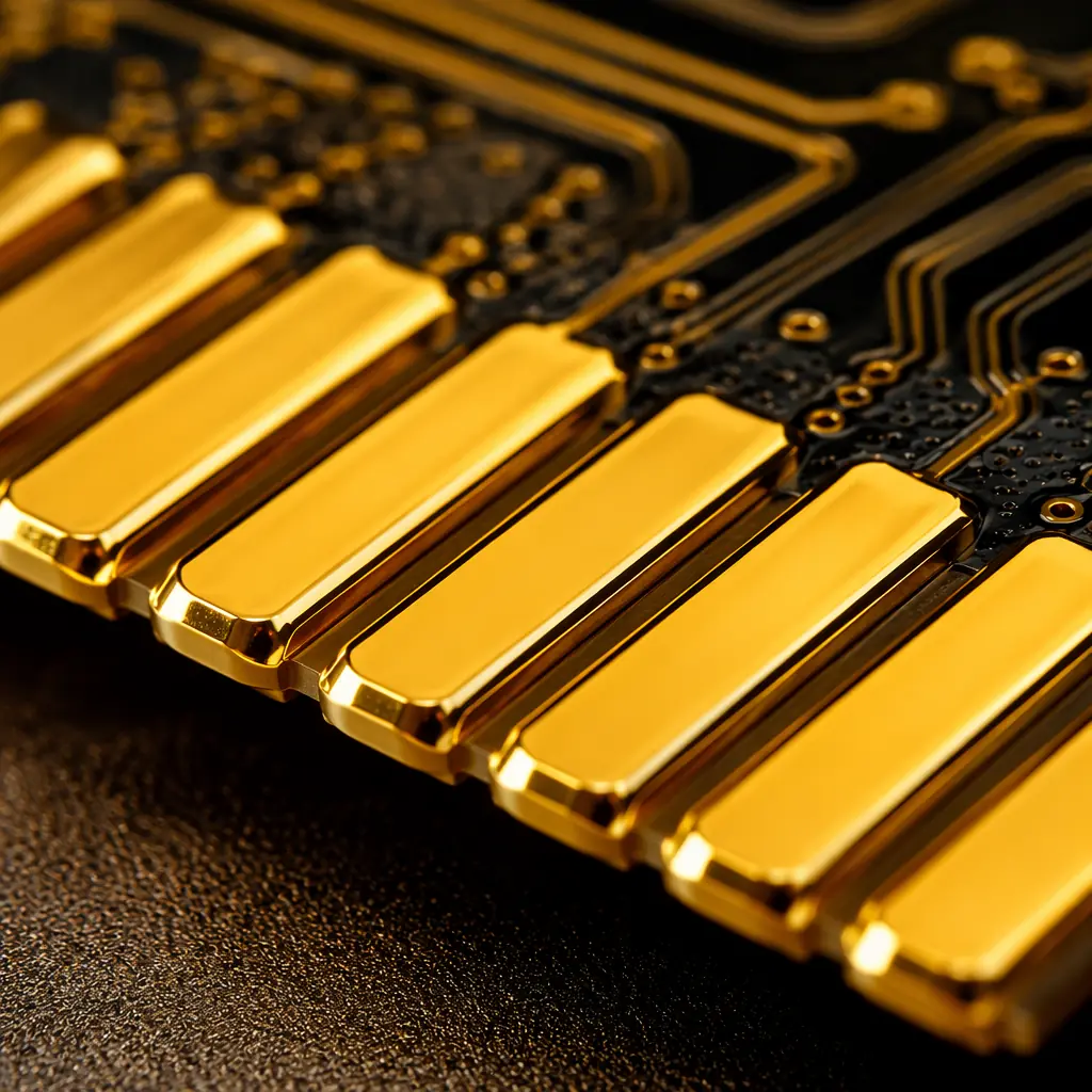
Gold plating on a PCB is not decorative, it's functional. It protects copper from oxidation, provides a solderable surface, and delivers the contact reliability needed for edge connectors that will be mated and unmated thousands of times. But "gold plating" is an umbrella term covering at least four distinct processes with dramatically different properties. Specifying "gold finish" without the details is like ordering "metal" for your car body, the outcome depends entirely on which metal and which process.
At Huaxing PCBA, we run 3 dedicated gold plating lines, electrolytic hard gold, ENIG (electroless nickel immersion gold), and ENEPIG, across our Shenzhen facility. This guide explains what differentiates hard gold from soft gold, when each is appropriate, and how to specify the right finish on your fabrication drawing so there are no surprises at incoming inspection. For the broader landscape of PCB surface finishes, see our complete surface finish selection guide.
Hard Gold vs Soft Gold, The Fundamental Difference
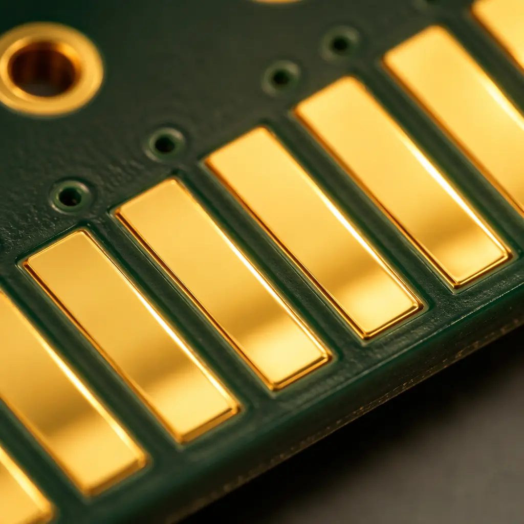
The distinction between hard and soft gold is not about the gold itself. Pure gold is always soft (25-65 HK Knoop hardness). The difference comes from what's alloyed with the gold and how it's deposited.
| Property | Hard Gold (Electrolytic) | Soft Gold (ENIG) | Soft Gold (ENEPIG) |
|---|---|---|---|
| Deposition method | Electrolytic (requires bus bar) | Electroless (chemical, no bus) | Electroless (chemical, no bus) |
| Gold purity | 99.7% Au + 0.3% Co/Ni hardener | ~99.9% Au (immersion) | ~99.9% Au (immersion) |
| Hardness (Knoop) | 130-200 HK | 60-90 HK | 60-90 HK |
| Typical thickness | 0.75-2.5 μm (30-100 μin) | 0.05-0.12 μm Au (2-5 μin) | 0.05-0.12 μm Au (2-5 μin) |
| Underlayer | 5-8 μm nickel (sulfamate bath) | 3-7 μm electroless Ni (6-10% P) | 3-7 μm electroless Ni + 0.05-0.3 μm electroless Pd |
| Wear resistance (mating cycles) | 1,000-10,000+ | <50 (not for connectors) | <100 (not for connectors) |
| Solderability | Poor (thick Au + Ni underlayer) | Excellent | Excellent (Pd barrier protects Ni) |
| Wire bondable (Al) | Yes (Type III, ≥0.75 μm) | No (too thin + Ni diffusion) | Yes (Pd layer is the bond surface) |
| Wire bondable (Au) | Yes | Limited | Excellent |
| Cost relative to HASL | 5-15× | 2-4× | 3-6× |
| Selective plating possible? | Yes (mask + plate specific areas) | No (full board immersion) | No (full board immersion) |
Procurement Rule of Thumb: If your PCB has edge connector fingers that will be inserted more than 50 times, you need hard gold, full stop. ENIG's 0.05-0.12 μm of soft gold wears through to the nickel underlayer within a few dozen mating cycles, creating a high-resistance NiO contact that causes intermittent failures. Hard gold at 0.75 μm survives 1,000+ cycles. That's the difference between a product that works for years and one that generates warranty returns in month three.
Hard Gold Plating, The Edge Connector Standard
Hard gold is electrolytic: the PCB panel is connected to a cathode bus bar, immersed in a gold plating bath (typically cobalt-hardened acid gold), and current is applied. This deposits a dense, wear-resistant gold-cobalt alloy (99.7% Au, 0.3% Co) over a nickel underlayer. The nickel provides the hardness foundation; the gold-cobalt alloy provides the corrosion-resistant sliding surface.
IPC-4552 classifies hard gold into three types based on thickness, each with distinct applications:
Type I, 0.75 μm (30 μin) minimum gold over 2.5 μm (100 μin) nickel
The general-purpose hard gold specification. Suitable for edge connectors with 100-500 design mating cycles, test points, and keypad contacts. This is what most commercial and industrial PCB edge connectors use. Cost adder vs HASL: approximately $15-25 per panel for selective edge plating on a standard 18×24-inch panel.
Type II, 1.25 μm (50 μin) minimum gold over 5.0 μm (200 μin) nickel
Specified for connectors expecting 500-1,000+ mating cycles. Common in telecom backplanes, military connectors, and test instrumentation. The thicker nickel underlayer resists cracking under repeated insertion forces. Our aerospace and defense PCB customers routinely specify Type II or Type III hard gold for connector cards that must survive the equipment's full service life without connector replacement.
Type III, 2.5 μm (100 μin) minimum gold over 5.0 μm nickel
The highest durability grade, used when the connector must survive 10,000+ mating cycles or when aluminum wire bonding is required. Type III is significantly more expensive (2-3× Type I) because the longer plating time reduces throughput, at our facility, a Type III panel spends roughly 45 minutes in the gold bath vs 12 minutes for Type I. Specify Type III only when the application demands it; over-specifying drives cost without adding functional value.
ENIG and ENEPIG, The Solderable Gold Finishes
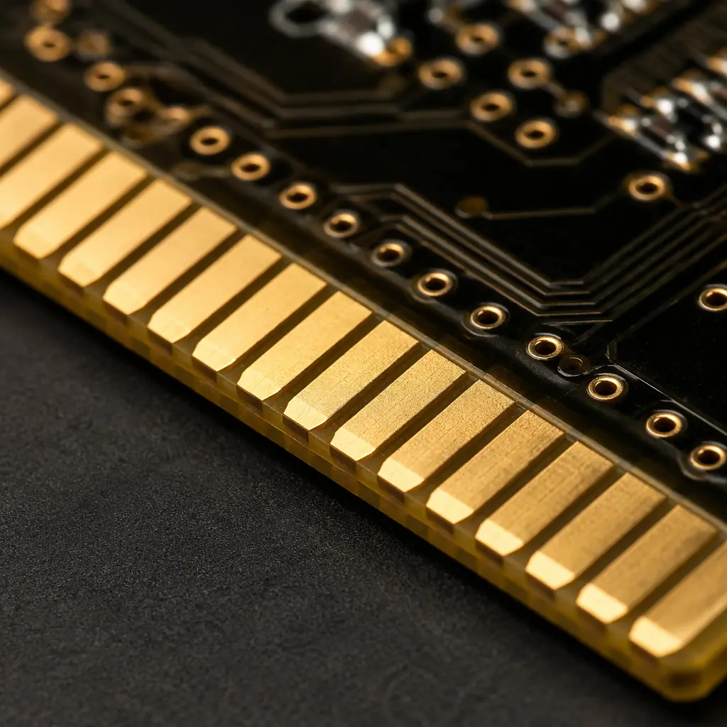
ENIG (IPC-4552A) deposits a thin immersion gold layer (0.05-0.12 μm) over electroless nickel (3-7 μm, 6-10% phosphorus). The gold's job is to protect the nickel from oxidation until soldering, during reflow, the gold dissolves into the solder and the joint forms between solder and nickel. This is fundamentally different from hard gold, where the gold remains as a sliding contact surface.
ENIG Advantages: Flat pads for fine-pitch, excellent solderability, 12-month shelf life
The electroless process produces exceptionally flat pads, critical for BGA and QFN packages where coplanarity matters. ENIG also provides the best shelf life (12+ months) among common finishes because the gold layer prevents nickel oxidation without passivating like OSP. For designs with fine-pitch BGAs, see our BGA assembly guide for finish compatibility details.
ENIG Limitation: Black pad syndrome and unsuitability for connectors
ENIG's main reliability risk is "black pad", excessive phosphorus enrichment at the Ni-Au interface that creates a brittle Ni₃P layer, causing pad cratering during drop testing. Modern ENIG processes (mid-phosphorus, 7-9% P) have largely solved this, but the risk remains if the plating bath chemistry drifts out of spec. ENIG is also entirely unsuitable for connector contacts, the 0.05 μm gold wears through almost immediately.
ENEPIG: The high-reliability upgrade with a palladium diffusion barrier
ENEPIG adds a thin electroless palladium layer (0.05-0.3 μm) between nickel and gold. This palladium layer acts as a diffusion barrier, it prevents nickel from migrating into the gold during storage, and it provides a superior surface for gold and aluminum wire bonding. ENEPIG is the finish of choice for medical device PCBs and semiconductor packaging where both solderability and wire bondability are required on the same board. For medical applications requiring ISO 13485 compliance, refer to our medical device PCB guide.
How to Specify Gold Plating on Your Fabrication Drawing
The most common error we see at Huaxing PCBA is ambiguous gold plating specifications. "Gold finish" or "gold plating on connectors" is not sufficient, it doesn't tell the fabricator which process, what thickness, or what underlayer. Here's how to specify correctly:
| Application | Specification to Write on Fab Drawing | IPC Reference |
|---|---|---|
| Edge connector, commercial | "Hard gold per IPC-4552 Type I, 0.75 μm Au min over 2.5 μm Ni, selective plating on edge contacts only" | IPC-4552 §3.2.1 |
| Edge connector, high-cycle | "Hard gold per IPC-4552 Type II, 1.25 μm Au min over 5.0 μm Ni, bevel edge 30° ±5°" | IPC-4552 §3.2.2 |
| Solder pads, fine-pitch | "ENIG per IPC-4552A, 0.05-0.12 μm Au over 3-7 μm electroless Ni (7-9% P)" | IPC-4552A |
| Wire bond pads + solder pads | "ENEPIG per IPC-4556, 0.05-0.12 μm Au / 0.05-0.3 μm Pd / 3-7 μm Ni" | IPC-4556 |
| Mixed: edge hard gold + ENIG pads | "Selective hard gold Type I on edge contacts (see detail A); ENIG per IPC-4552A on all SMD pads" | IPC-4552 + IPC-4552A |
Cost Warning: Selective hard gold + ENIG on the same board requires two separate plating processes (electrolytic gold for edge connectors, then mask, then ENIG for pads). This adds $30-50 per panel and 1-2 days to lead time versus single-finish boards. If your design can avoid mixed finishes, do so. If it can't, budget the extra cost and lead time into your procurement plan, do not expect standard ENIG pricing.
Gold Plating Quality Control, What to Check at Incoming Inspection
When you receive gold-plated PCBs, three measurements separate acceptable product from latent field failures:
XRF thickness measurement, non-negotiable for every lot
An X-ray fluorescence (XRF) analyzer measures gold thickness non-destructively in seconds. For hard gold PCBAs, our IQC process samples 5 points per panel and rejects any lot with a single measurement below the minimum specified thickness. Gold at 0.6 μm instead of 0.75 μm may look identical but will wear through in half the cycles.
Porosity test for hard gold (nitric acid vapor per ASTM B735)
Porosity in the gold layer exposes the nickel underlayer to the atmosphere, causing NiO formation that increases contact resistance. The nitric acid vapor test exposes any pores: nickel corrodes through pores and stains the gold surface. For Type II/III hard gold connectors, specify "Porosity Class A per ASTM B735" on your procurement document.
Solderability test per J-STD-003 for ENIG/ENEPIG pads
Immersion gold that's too thin (<0.03 μm) allows nickel oxidation before soldering. J-STD-003 dip-and-look testing catches this. At Huaxing PCBA, we perform solderability coupons on every ENIG batch. A quick dip in SAC305 solder at 255°C must produce >95% wetting. Batches below 90% are re-plated. For an overview of all PCB testing methods, see our testing methods comparison.
Gold plating is one of the few PCB manufacturing processes where the difference between "works" and "fails in the field" is measured in microns. Specify the process, the thickness, and the acceptance criteria, and verify with XRF at receiving inspection. At Huaxing PCBA, our process engineers certify every gold-plated lot with thickness reports and porosity test results before shipment, so your IQC team knows exactly what arrived.
