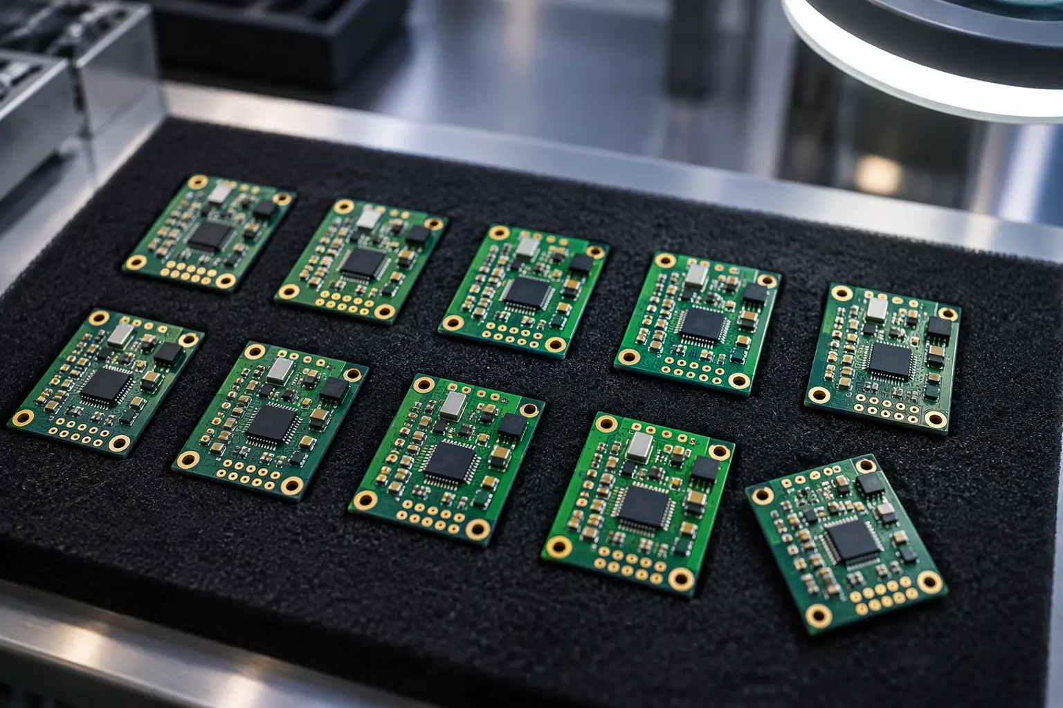
On 9 November 2026 Anthropic published a research note titled Claude can design electronic prototypes from start to finish. The claim is specific and testable: given a one-sentence requirement, the model wrote specifications, drew schematics, placed components, routed copper, modelled printable enclosures and wrote firmware for three devices — a USB speakerphone, a voice-assistant hub and a handheld virtual pet. A partner company, Diode, fabricated the boards directly from the model's output files. Their team reported that the usual rounds of manufacturing changes did not happen.
Read carefully, that is a statement about a prototype. The article says so itself: the devices have not been through electrical validation, antenna tuning, thermal testing or certification, were not designed for mass production, and the partner has a commercial relationship with Anthropic. The claim is narrow, and it holds.
What the article does not address is the position this puts a fabricator and assembler in. For twenty years the person sending us Gerbers was a hardware engineer who had already made a hundred judgement calls that do not appear on the drawing. When the files come from an AI agent, some of those calls were made and some were not, and the two are indistinguishable at a glance. The factory becomes the last reviewer in the chain, sometimes the only one.
What Actually Changed, and What Did Not
If you have read anything about AI in electronics design before 2026, put it aside. The previous generation of claims was about narrow optimisers: a tool that suggested a better component placement from a fixed netlist, or a router that finished a board a human had begun. Those tools assumed the difficult decisions were already made and were being handed to an algorithm for refinement.
The 2026 claim is different in kind. Placement, routing, stackup choice, mechanical fit and firmware were all produced from a single requirement statement with minimal prompting. The reported improvement is measurable rather than rhetorical: on Diode's internal PCB Gym benchmark, which strips the layout from a finished board and asks a model to rebuild it, the current model scored 69% against 25% for the model a generation earlier. On the public BenchCAD 2.1 benchmark for reconstructing boards from engineering drawings, it scored 83.5%, close to double its predecessor.
What did not change is the part where a factory earns its money. A board that routes cleanly can still be unbuildable at your process capability, unsellable because a part has no second source, uncertifiable because a ground plane is severed under a connector, and unrunnable because the firmware assumes a rail that no regulator on the board can hold. Those are not design errors in the CAD sense. They are manufacturing and compliance facts, and they are established on the floor, not in the model.
Short answer: an AI design package gets you a technically valid schematic and layout much faster than a drafting department, and it gets you nothing you can ship. Production adds five things the design file cannot contain: process-capability DFM against a specific factory, a committed BOM with second sources, impedance and stackup re-derivation from a real laminate, a documented change history, and certification evidence. The design is the cheap part.
| Stage | Who Owns The Decision | What It Costs If It Is Wrong |
|---|---|---|
| Prototype layout | AI agent, reviewed by a human | One board spin, days |
| Process-capability DFM | Fabricator's process engineer | Lot scrap or a re-quote after order |
| BOM and sourcing | Purchasing plus design owner | Line stop, or a redesign at the last minute |
| Stackup and impedance | Fabricator, from the actual laminate | Signal integrity failures found in test |
| Certification | Accredited lab, on the finished unit | 6-14 weeks and a full retest cycle |
What an AI-Authored Design File Reliably Gets Right
Our intake experience over the last quarter is more positive than the sceptical version of this story suggests. Files generated by agents are, on average, cleaner than files from a small in-house team working under deadline. Four things are consistently good.
Netlist consistency. Schematic and layout agree. The classic failure of a rushed human design — a part renumbered on one side and not the other, leaving a footprint whose pads connect to the wrong net — essentially does not occur, because both sides are generated from a single representation.
Rational placement. Supporting parts sit near the IC they serve. Decoupling capacitors are close to the pins they decouple, which is the single most common thing a human layout gets wrong under time pressure. Bulk capacitance is grouped sensibly. Connectors are oriented so cables approach them from the board edge rather than across it.
Ordered routing. High-speed pairs are routed first, kept equal length, and given the correct differential spacing. Impedance-sensitive nets do not get routed last around obstacles. In one published example the agent routed one pair at a time through a 100-pin connector fanout rather than letting a batch router optimise globally, which is what an experienced engineer does and what a push-button router usually does not.
Self-correction. When a layout cannot be completed, current models notice and change the plan rather than leaving a board at 95% routed and calling it done. The published examples show signals reassigned to interchangeable pins, whole corners of a board re-laid, and traces ripped out and re-routed dozens of times. Older models produced the 95%-and-unusable boards that Diode reported they could not build.
None of this is a reason to skip review. It is a reason to review a different list, because the faults cluster differently than they do in human files.
What These Files Systematically Miss
Six things recur. Each is invisible in a CAD viewer, and each has cost us a re-quote or a lot hold at least once.
1. Fabrication data hygiene. Exported Gerbers from an agent-driven session almost never carry X2 attributes: no net names on copper layers, no component references attached to pads. The board still etches correctly. What is lost is the ability to run a net-aware electrical test from the Gerber alone, which moves part of the test-program burden back to the customer or to us. It is fixable, and it has to be noticed before the panel is released.
2. Stackup and impedance are asserted, not derived. A design may specify 50 Ω single-ended and 100 Ω differential traces. The number in the file is a target. The actual impedance depends on the laminate the factory stocks, the prepreg thickness it actually gets from the supplier this month, the copper weight after plating and the soldermask thickness. We re-derive it with a field solver against a real stackup, and the trace widths that come back are frequently 8-15% different from the ones in the design file. On a two-layer board this rarely matters. On a six-layer board with USB 3 or Ethernet pairs, it is the difference between passing eye-diagram limits and not.
3. Process-capability margins versus rule-checker margins. A DRC pass means the layout obeys a rule set, usually a generic one. Our process capability is specific: minimum soldermask sliver, minimum annular ring, minimum clearance at the copper weight being used, minimum hole-to-copper for the drill class. A design can pass its own DRC and still contain six slivers below our minimum. The published example shows the agent catching and fixing exactly this class of issue itself, which is good, and also shows why the check has to be repeated against the receiving factory's numbers rather than a default set.
| Feature | Typical AI File Value | Process Minimum At 1 oz | Consequence |
|---|---|---|---|
| Soldermask sliver | 0.08-0.10 mm | 0.10 mm (0.08 mm at 0.5 oz) | Mask lift, bridging risk |
| Annular ring, Class 2 | 0.05 mm | 0.05 mm absolute | Breakout on drill shift |
| Annular ring, Class 3 | 0.05 mm | 0.05 mm plus breakout allowance | Fails IPC-6012 Class 3 |
| Silkscreen to pad | 0 mm overlap | 0.15 mm | Legend on pad, solderability |
4. BOM commercial reality. A parts list can be electrically correct and commercially unusable. Lifecycle status, second sources, minimum order quantity, and whether the exact package and temperature grade are actually on the shelf this week are not determined by the design. Neither is the assembly question the customer usually has not considered: whether the parts are available in the reel format and quantity the line needs, or only as cut tape.
5. Change history and revision control. A design that was re-routed dozens of times during generation has a rich history that does not survive export. What arrives is a final snapshot. For a prototype that is fine. For anything that will be built twice, the absence of a revision trail means the second order cannot be proven identical to the first, and a customer cannot answer a question about why a board changed between builds.
6. The certification assumption. This is the largest one. Nothing in a CAD file indicates whether the finished product will pass emissions testing. The published research is explicit that its prototypes were not certificated. A board can be perfectly manufacturable and still fail a CISPR 32 radiated emissions scan because of a switching regulator's layout, a cable-entry filter that was never fitted, or a clock trace that runs to the board edge. Certification is a property of the finished assembly in an enclosure, tested in an accredited chamber, and it takes 6-14 weeks to book and complete for a first submission.
The Five Gates We Run On A Submitted Design
This is the practical content of the page. Whether the files came from an agent, a contractor or your own team, the sequence is the same. What changes is which gates produce findings.
Gate 1 — Data integrity, same day. We check that every layer is present and in the correct polarity, that the drill file and the copper agree, that the board outline closes and matches the panel, and that net-aware attributes exist. Missing X2 attributes are regenerated if a netlist is supplied. A four-layer prototype board clears this gate in one working day, which is what our published DFM turnaround is based on. A design that arrives with a broken outline or a drill file in the wrong units stops here regardless of how good the layout is.
Gate 2 — Process-capability DFM against our numbers. Not a generic DRC. We run the design against the capability of the specific line that will build it: minimum feature at the copper weight specified, annular ring by IPC class, soldermask and legend clearances, hole-to-copper, panel utilisation and the effect of the chosen surface finish on minimum pad spacing. Findings are sorted into must-fix and advisory, with the must-fix list written in terms of the geometry, not the tool's message text.
Gate 3 — Stackup and impedance re-derivation. We propose a stackup from laminate actually in stock and compute the trace geometry that meets the design's impedance targets on that stackup. The customer approves the stackup, then we hold the approved impedance geometry as a manufacturing constraint on the order, so a later laminate substitution cannot silently change the electrical result.
Gate 4 — BOM and assembly feasibility. Every line checked for lifecycle status, stock at the time of order, package and temperature grade, and availability in the feed format the line requires. Where a part is single-source or has a long lead time, we report it with the cost of the alternatives rather than substituting quietly. This gate is where most schedule surprises are found, and where they are cheapest to fix.
Gate 5 — Design-for-test and first-article plan. Test coverage decided before the panel is released: which nets are probed, whether a fixture is needed and at what cost, and what the first-article inspection will measure. This is the gate that turns a working prototype into something that can be built again with the same result.

Prototype and Production Are Not the Same Problem
The single most useful distinction for anyone starting from an AI-generated design is how the gates change when quantity changes. A design that clears three gates at prototype volume may need all five, plus a tolerance study, at volume.
| Gate | Prototype (1-10 pcs) | Production (500+ pcs) |
|---|---|---|
| Data integrity | Layer check, netlist regenerated | Plus revision lock and panel-level net-aware test |
| Process DFM | Must-fix geometry only | Plus panel utilisation, yield estimate, tolerance stack |
| Stackup | Stock laminate, impedance approximated | Impedance coupons on the panel, measured and reported |
| BOM | Stock at time of order | Second source qualified, lifecycle and last-time-buy assessed |
| Test | Functional check by hand | Fixture, coverage statement, FPY target |
| Certification | Not applicable | 6-14 weeks, must be planned before the design is frozen |
The row that catches the most projects is the last one. Teams spend a month shortening the design phase and then discover the certification cycle is the real critical path. If the product has a radio, a mains connection or sells into a regulated market, the certification path should be scoped at the same time as the schematic, not after the first article works.
Ten Questions To Ask Before You Fab
Ordered by the cost of getting the answer wrong. Ask them of the design owner, and ask them of the factory.
1. Who holds the intellectual property in this design, and is that written down? An agent output that was trained commercially and produced under someone's account has an unclear provenance until the terms are read. It matters at funding, at acquisition and in a dispute.
2. Which IPC class is this board specified to, and does the annular ring match it? Class 2 and Class 3 differ in the breakout allowance, and the difference shows up as a rejection at final inspection.
3. What copper weight and what laminate will the board actually be made from, and who approved that stackup? If the answer is "we will see what is in stock", the impedance numbers in the design file are decorative.
4. Are the Gerbers exported with net attributes, and is a netlist included? Without them, net-aware test from the artwork alone is limited.
5. Which nets are impedance-controlled, and has the geometry been computed on the proposed stackup rather than assumed?
6. How many BOM lines are single-source, and what is the longest lead time among them? The second question determines the schedule more often than the design does.
7. Can the design be built at the quantity you intend, on the process the factory will assign it to? A design that is comfortable at prototype quantities may need panel-level changes at volume.
8. What is the test strategy, and what does the fixture cost if one is needed? Fixture NRE is often a five-figure line item that appears after the design is already frozen.
9. Which certifications are in scope, and has the market entry date been set against the certification lead time rather than the design date?
10. If a part disappears between the first build and the second, who decides the replacement and who re-validates? A second source that was never qualified is not a second source.
When An AI Design Is The Wrong Starting Point
Three cases. We turn projects away at intake in each of them, and it is cheaper than taking them.
Anything that ships with a radio and a metal enclosure. Antenna performance depends on the enclosure, the ground plane and the hand of the user. A layout that is geometrically valid can put an antenna 2 mm from a battery shield and lose 6 dB of efficiency. Antenna tuning requires measurement on the finished assembly; a design file cannot substitute for it, and the retest cycle is where the schedule goes.
High-current power and mains-adjacent boards. Clearance and creepage are compliance requirements, not layout preferences. The failure mode is not a dead board; it is a product that fails a safety review after tooling has been paid for.
Anything for which nobody can sign a declaration. Regulated markets require a legal person to attest to the design. An agent cannot be that person. If the customer has not read their own design package and cannot answer why a component was chosen, the first failure analysis becomes an argument about responsibility rather than an engineering task.
In every other case the practical position is that an AI-generated design is a normal starting point, reviewed on the same gates as any other incoming work, with the difference that we look harder at provenance, stackup derivation and certification scope, because those are the three things a capable generator does not know about your factory or your market.
The wider effect on this industry is worth stating plainly. If a design package that used to take three weeks now takes a day, the volume of design work rises and the volume of fabrication follows it. The constraint moves from drawing boards to process capability, second sources and test chambers — which is where a factory's actual assets sit. That is a better position for a manufacturer than the one it had when the drawing was the bottleneck, and it makes the first review gate the most valuable thing we do for a new customer. For the review methodology behind those gates, see the DFM checklist buyers actually use, and for how we handle stackup selection in practice, stackup design and impedance control. The assembly-side counterpart is covered in shift-left DFM verification for PCBA, first-article approval in first article inspection (FAI), and the certification timeline in UL certification for PCB manufacturing.