
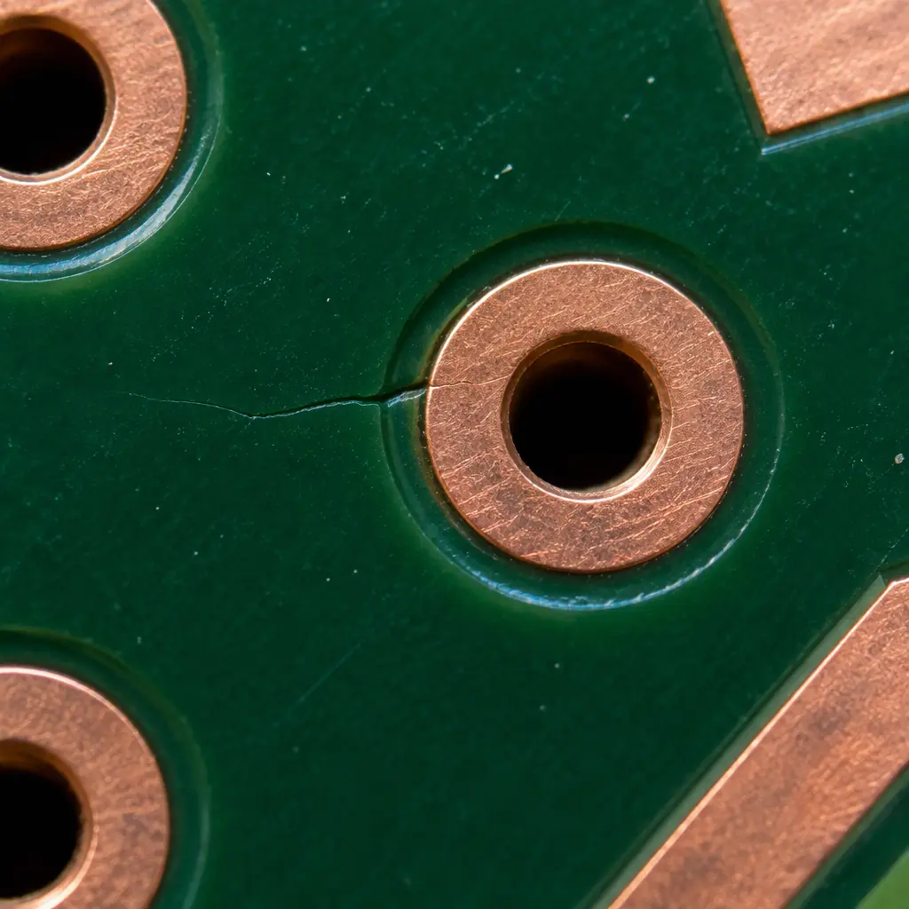
Pad cratering is one of the most misattributed failures in electronics assembly. A board comes back from a drop test or a field return with a component detached, the fracture surface sits at the pad, and the immediate assumption is a soldering problem — a cold joint, a poor reflow profile, a contaminated pad. The assembly house adjusts the oven, re-runs the lot, and the problem returns, because the failure was never in the solder. It was in the laminate underneath the pad, where a crack propagated through the epoxy resin that anchors the copper pad to the board.
Understanding pad cratering means understanding that the pad is not just a metal feature sitting on an inert substrate — it is a copper island bonded to a resin matrix, and the strength of that bond is finite. When a solder joint transfers mechanical load into the pad, the weakest link can be the resin rather than the solder, and the resulting crack runs through the laminate, taking the pad with it. This guide covers what pad cratering is, the thermal, mechanical and material drivers behind it, how to detect it with the right methods, and the design and material levers a designer actually controls. At Huaxing PCBA we run assembly and laminate selection under IATF 16949 and ISO 9001, and pad cratering is a review point in our DFM process for high-reliability designs.
What Pad Cratering Actually Is
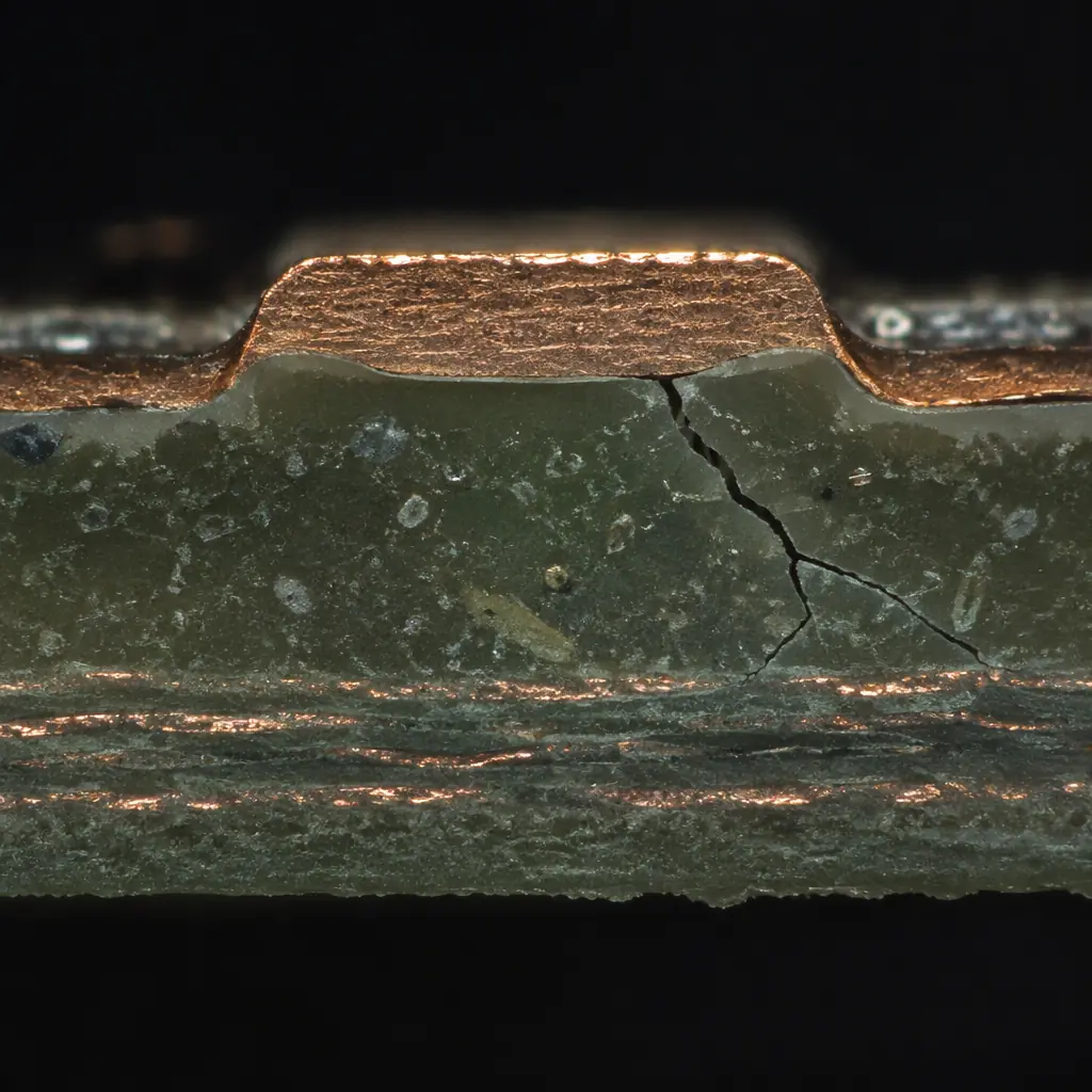
Pad cratering is a fracture that initiates in the laminate — the epoxy/glass composite — at the perimeter of a copper pad, and propagates beneath the pad. The copper pad itself remains intact; what fails is the resin that holds it. The crack typically starts at a corner or edge of the pad, where the copper-to-resin interface sees the highest stress concentration, and runs parallel to the board surface under the pad. In severe cases the pad and the solder joint separate from the board as a unit, but the fracture surface is in the resin, not at the solder interface.
The distinction matters enormously for diagnosis. A solder-joint fracture means the joint failed. A pad crater means the board failed. The two have different root causes and different fixes, and a corrective action aimed at the wrong one will not resolve the failure. Pad cratering is most common on lead-free assemblies and on thin boards or pads bonded to laminate with lower mechanical strength, and it is a known interaction with the higher temperatures lead-free reflow demands.
Key Takeaway: Pad cratering is a laminate failure, not a solder failure. If a detached component leaves resin residue on the underside of the pad or a crater-shaped depression in the board, the root cause is material, design or thermal history at the board level — not the reflow oven alone.
What Causes the Resin Crack
Pad cratering results from the combination of mechanical stress at the pad and reduced resistance of the laminate to that stress. Three categories of driver interact.
Thermal drivers. Lead-free reflow runs hotter — peak temperatures of 235–250°C versus around 210–220°C for tin-lead. Every reflow cycle subjects the laminate to thermal expansion, and the mismatch in expansion between the copper and the resin creates stress at the pad perimeter, especially at the pad corners. Multiple reflow cycles (double-sided assembly, rework) compound this. Absorbed moisture released rapidly during reflow — a phenomenon known as popcorning at the board level — can further weaken the resin around the pad. A laminate that is marginal at lead-free temperatures can pass at tin-lead and crater at lead-free without anything else changing.
Mechanical drivers. Any load that bends the board or pulls on the joint transfers stress to the pad. This includes depaneling stress if boards are separated with excessive flexing, board-level handling and depanel, connector insertion and removal forces, board flexure during test and in the housing, and — critically — drop and shock events. Larger components and heavier parts exert more load, and the pad edge is where the resin sees the highest stress concentration regardless of the load direction.
Material drivers. The laminate's mechanical properties set the baseline resistance. Higher glass-transition temperature (Tg) and higher decomposition temperature (Td) laminates generally resist cratering better, because they retain stiffness and bond integrity at higher temperatures. Resin systems differ in their adhesion to copper — the pad-to-resin bond strength is the property that ultimately decides cratering resistance. Filler content and resin formulation matter as much as the headline Tg figure. Pad geometry and the presence or absence of features that reduce the copper-to-resin contact area also change the stress concentration at the pad edge. This is closely related to the material selection decisions covered in our PCB materials guide.
Pad Cratering vs Solder-Joint Fracture
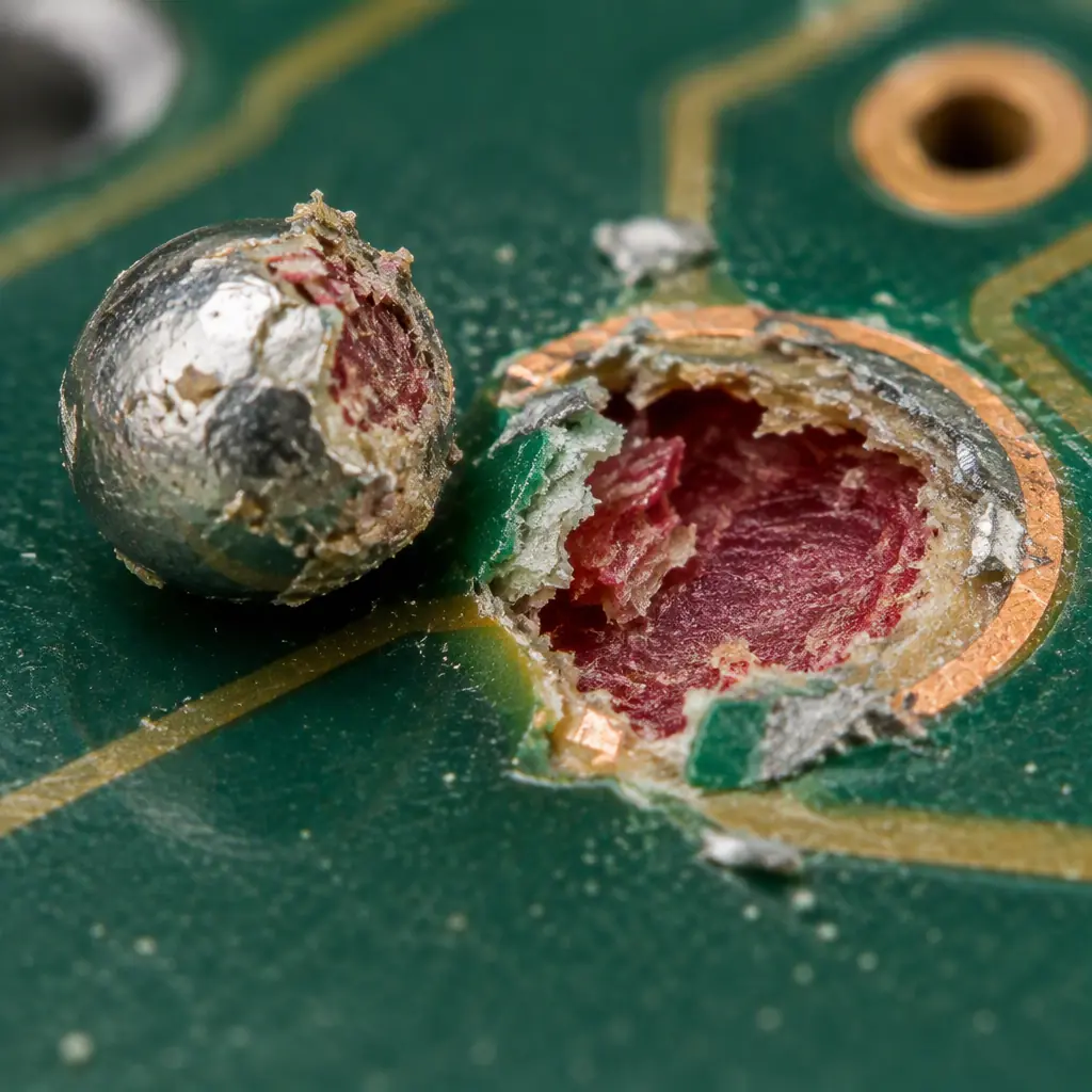
Telling the two apart is the first step of any investigation, and it can be done by inspecting the fracture surfaces and, where needed, by cross-sectioning. In a solder-joint fracture, the separation occurs within the solder or at the intermetallic interface, and the pad remains attached to the board with its plating intact. In pad cratering, the fracture surface reveals resin — fibers, filler and epoxy — and the pad often carries a layer of laminate with it.
At the board side, a crater leaves a shallow depression where the pad used to be, bounded by the remains of the resin. A small magnifier and good lighting will show this to a trained eye, but the definitive evidence comes from cross-sectioning, which reveals the crack running through the resin beneath the pad rather than through the joint. Misreading a crater as a joint failure leads to changes in the reflow profile that do nothing, because the thermal history was only one contributor and frequently not the dominant one.
Two other failure modes are sometimes confused with pad cratering. Pad lifting is a separation at the copper-to-laminate interface caused by mechanical force during assembly or rework, generally without the resin cracking under the pad. Board-level delamination is a separation between laminate layers, driven by moisture and thermal stress, and shows as a blister or separation across a wider area rather than at a single pad. The location and the breadth of the separation distinguish them from cratering, which is localised to the pad and contains a resin crack rather than a layer-to-layer split.
Detection: Dye-and-Pry and Microsection
Because pad cratering is hidden under the pad, detection requires either mechanically exposing the fracture or cutting through it. Two methods dominate.
Dye-and-pry. The assembled board is submerged in a penetrating dye under vacuum so the dye enters any existing cracks, then the component is pried off, and the fracture surfaces are examined for the dye. Dye present under the pad confirms a fracture there and shows its extent, and the pattern of dye on the pad and board side indicates whether the crack is in the solder, at the interface, or in the laminate. Dye-and-pry is a destructive but relatively fast and low-cost method, well suited to comparing designs or process variants because it lets a batch of samples be tested in a reasonable time.
Microsection. A cross-section through the joint and pad, examined under a metallurgical microscope, shows the crack path directly. This is the definitive method: it reveals whether the fracture is in the solder, the intermetallic layer, the copper-to-resin bond, or the resin beneath the pad. Where the crack path is ambiguous on a single section, a series of sections through the pad corner — where cratering usually starts — resolves it. Our guide to microsection analysis covers how these sections are prepared and read, and the general discipline is shared with the wider class of defects described in PCB solder joint defects.
For a design or process qualification, dye-and-pry on a batch of samples establishes the failure rate and location across the population, while microsection on selected samples confirms the mechanism. Used together they give both the statistical and the metallurgical picture, which is what a corrective action needs to be aimed correctly.
Design and Material Levers That Prevent It
Because pad cratering is a board-level failure, the levers that prevent it sit with the designer and the material selection rather than with the assembly process alone. The following are the ones with the greatest effect.
Choose a laminate with adequate Tg and Td
Higher-Tg, higher-Td materials resist the thermal stress of lead-free reflow. Do not select laminate on cost alone for a lead-free, high-reliability design.
Control pad geometry and size
Larger pads increase the copper-to-resin interface and can raise stress concentration. Keep pads to the minimum that satisfies the solder-joint requirement.
Avoid features that reduce bond area
Via-in-pad and large thermal-relief openings under a pad reduce the resin contact area and mechanically weaken the pad. Manage them deliberately.
Keep reflow cycles and thermal exposure to a minimum
Double-sided assembly and rework add thermal cycles. Once a design is qualified, avoid adding unnecessary reflows.
Reduce mechanical stress at the pad
Depanelisation without flexing, careful handling, and lower connector insertion forces all reduce the mechanical load that initiates the crack.
Control moisture before reflow
Bake moisture-sensitive boards before assembly where storage or transport may have allowed absorption, to reduce thermal-stress popcorning at the pad.
Key Takeaway: Pad cratering is prevented primarily by laminate and pad design, not by reflow tuning. Select a higher-Tg laminate for lead-free high-reliability work, minimise pad size and bond-area-reducing features, and control the mechanical stress the board sees during depaneling, handling and use.
Incoming and Process Controls for Buyers
For a buyer, pad cratering is managed by writing the right requirements and verifying them rather than by inspecting for it after the fact. The laminate specification should name the material family with a Tg and Td suitable for the process, not simply "FR-4." The assembly specification should limit reflow cycles where reliability is critical, and require moisture control (baking) for moisture-sensitive parts. For high-value or high-reliability designs, a drop-test or board-flex qualification that includes failure analysis — dye-and-pry or microsection — turns pad cratering from a field surprise into a pre-production finding.
It is also worth reviewing the board design for the geometry that concentrates stress at the pad: oversized pads, pads with large openings beneath them, and connectors that see repeated insertion cycles. These are the locations where cratering will appear first if it appears at all, and a targeted reliability test at those locations is more efficient than testing the whole board. The same sample-preparation discipline that reveals cratering overlaps with the general reliability testing framework described in our guide to microsection analysis and the materials guide.
At Huaxing PCBA we select laminates to suit the assembly process and reliability class, and pad cratering is a review point in our DFM process for lead-free and high-reliability designs, with dye-and-pry and microsection available for qualification. Send your Gerber files with the reliability requirement and operating environment and we will recommend an appropriate laminate and return a quote inside 24 hours with a free DFM review, or talk to our engineering team about pad cratering risk on a lead-free high-reliability design.
