
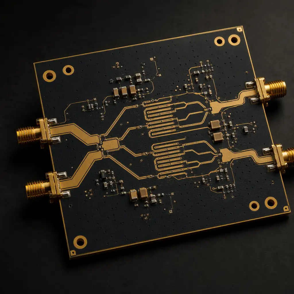
PCB Types / RF / Microwave PCB
RF and microwave PCBs demand exacting impedance control, low-loss laminates, and precision copper etching. Our RF capability spans Rogers 4350B, 4003C, RT/duroid 5880, and Taconic PTFE, with ±5% impedance tolerance verified by TDR on every panel.
Technology Overview
RF and microwave PCBs operate at frequencies where every millimeter of trace is a transmission line. Unlike digital PCBs where signals are simply "on" or "off," RF boards must manage impedance, phase, insertion loss, and return loss across the entire signal path. The choice of laminate, its dielectric constant (Dk) and dissipation factor (Df), is the single most critical design decision.
We stock and regularly process Rogers 4350B, 4003C, RT/duroid 5880, 5870, RO3003, RO3010, RO4835, and Taconic RF-35, TLX, TLY, as well as Arlon and Isola Astra MT77. For cost-optimized designs, we offer hybrid stackups, RF laminate on outer layers bonded to FR-4 cores.
Technical Specifications
| Laminate Portfolio | Rogers (4350B, 4003C, RO3003, RO3010, RO4835, RT/duroid 5880/5870) · Taconic (RF-35, TLX, TLY) · Arlon · Isola (Astra MT77) · PTFE · LCP |
| Dielectric Constant (Dk) | 2.20 – 10.2 across material portfolio |
| Dissipation Factor (Df) | As low as 0.0009 @10GHz (RT/duroid 5880) |
| Max Frequency | 77 GHz (mmWave radar); standard RF to 20 GHz |
| Number of Layers | 2 – 16 (pure RF); up to 24 with hybrid FR-4; up to 40 evaluation |
| Min. Trace / Space | 4 / 4 mil (0.1 / 0.1 mm) on Rogers; 3/3 mil on hybrid FR-4 layers |
| Impedance Control | ±5% (single-ended 50Ω); ±7% (differential 100Ω); TDR verification |
| PCB Thickness | 0.2 – 3.2 mm (RF core); thicker with hybrid build-up |
| Surface Finish | Immersion Silver (recommended for RF) · ENIG · ENEPIG · OSP |
| Solder Mask | Green / Blue; no mask on RF traces recommended; selective mask opening |
| Copper Weight | 0.5 – 2 OZ (18-70µm); ED or RA; HVLP ultra-smooth for mmWave |
| Quality Standard | IPC-6012 Class 3 · IPC-6018 (microwave) · IATF 16949 · ISO 9001 |
Workhorse RF laminate. Good balance of performance and processability. Compatible with standard FR-4 processes, no special PTFE treatment needed. Ideal for cellular base station, power amplifier, and general RF to 20GHz.
Lowest Dk and Df in the portfolio. Pure PTFE composite with micro-fiberglass reinforcement. Requires plasma treatment for PTH. Used in millimeter-wave, satellite communication, and phased-array radar.
Ceramic-filled PTFE designed for 77GHz automotive radar and 5G mmWave. Excellent Dk stability over temperature. Available in thin cores down to 5 mil (0.127mm). Preferred for 24/60/77GHz antenna arrays.
Rogers laminate on outer layers with standard FR-4 cores. Achieves RF performance where it matters while using low-cost FR-4 for power/ground planes. Most common in 5G CPE, WiFi 6E/7 routers, and IoT gateways.
Manufacturing Process
PTFE-based laminates require specialized processing: plasma treatment for PTH hole-wall activation (conventional desmear won't work on PTFE), controlled drill parameters to avoid smearing, and careful copper surface preparation. Every RF panel is TDR-tested for impedance at multiple coupon locations.
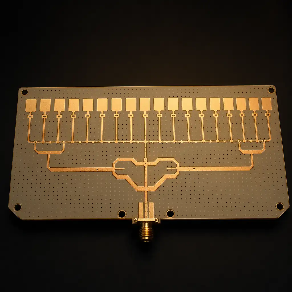
Base station PA, massive MIMO antenna, backhaul radio
77GHz radar, blind-spot detection, adaptive cruise control
LEO satellite transceiver, phased-array, ground terminal
Tri-band router, mesh AP, 6GHz front-end module
Electronic warfare, SIGINT receiver, missile seeker
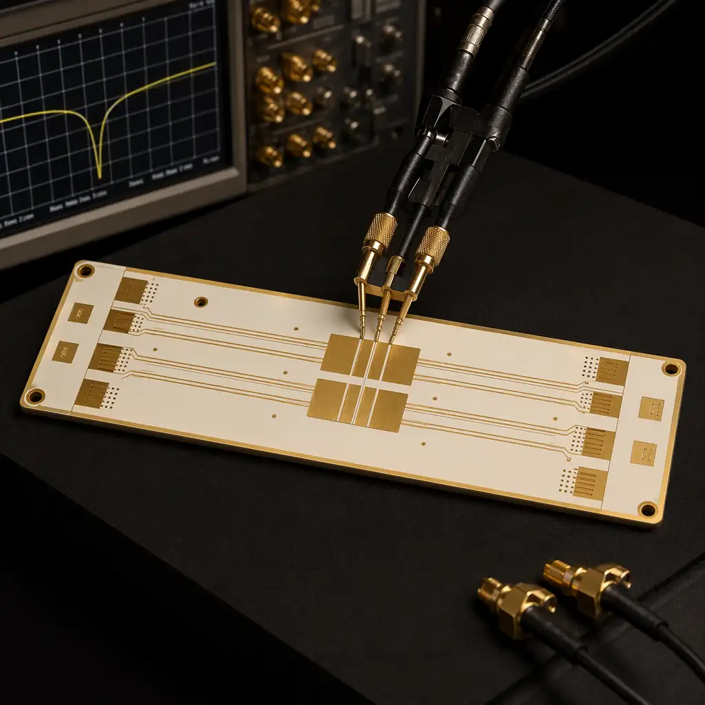
VNA test fixture, probe station cal substrate, RF switch matrix
Tell us your frequency, laminate preference, impedance targets, and layer count. Our RF engineering team will review your design for free and provide a detailed quote within 24 hours.

Tell us frequency, laminate, impedance targets, and quantity. Free review within 24h.