

Got Questions?
28 detailed answers from our engineering and sales teams. Don't see yours? Reach out directly.
Our MOQ is 1 piece for PCB fabrication and 5 pieces for PCBA. We specialize in supporting both prototyping and mass production, same factory, same quality standards. For prototypes, we recommend ordering 5–10 pieces to validate your design before scaling to production volumes.
Standard quote turnaround is within 24 hours. For simple 2-4 layer PCB orders with complete Gerber files, we often respond within 4–6 business hours. Complex multilayer or PCBA orders with BOM review may take the full 24 hours. Use our online estimator for instant ballpark pricing.
We accept T/T (wire transfer), L/C (Letter of Credit), PayPal, and Alibaba Trade Assurance. For new clients, we typically start with 50% deposit / 50% before shipment. After establishing a relationship, we offer net-30 terms for qualified buyers.
PCB pricing depends on: layer count, board dimensions, quantity, material (FR-4 vs. Rogers vs. ceramic), copper weight, surface finish, trace/space requirements, and turnaround time. Engineering/NRE fees are one-time and decrease per unit with volume. Our online calculator gives instant estimates, try different configurations to see how each parameter affects price.
We don't offer free samples for custom PCB fabrication, but we do offer heavily discounted prototype pricing for first-time customers: typically 30-50% off standard prototype rates on your first order. This includes full DFM review, AOI, and electrical testing, identical to our production QC process.
Yes. Once we've manufactured your design, NRE and tooling fees are waived on re-orders (files are kept on file for 3 years). Re-orders also benefit from faster turnaround since CAM engineering is already complete. We maintain your approved production panel layout and test fixtures for consistent quality across batches.
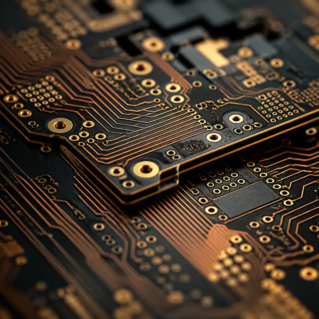
We manufacture up to 32 layers for rigid PCBs. Our high-layer-count capability includes blind, buried, and back-drill vias, with precision impedance control (±5%). For HDI designs, we support any-layer microvia technology with laser-drilled vias down to 0.075mm.
We stock FR-4 (standard, high-Tg, halogen-free), Rogers (4350B, 4003C, 3003), Taconic (RF-35, TLX), Isola (370HR, FR408HR), Panasonic Megtron 6, Polyimide (flex/rigid-flex), Aluminum (MCPCB), Copper-core, Al₂O₃ and AlN ceramic. For materials not in stock, procurement lead time is typically 3–7 days. We can source virtually any laminate, just ask.
We offer: ENIG (electroless nickel immersion gold), ENEPIG, HASL lead-free, OSP, Immersion Silver, Immersion Tin, and Hard Gold (for edge connectors). ENIG is our most popular finish, excellent solderability, flat surface for fine-pitch components, and 12+ month shelf life. See our PCB fabrication page for a full finish comparison.
Our standard capability is 3/3 mil trace/space with 0.15mm minimum mechanical drill. For advanced designs, we achieve 2.5/2.5 mil and 0.10mm laser drill. We recommend staying at 5/5 mil or above for cost-optimized production. All trace/space values are verified during DFM review against your target IPC class.
Yes, impedance control to ±5% tolerance is a standard offering. We use Polar Instruments Si8000 for stackup simulation before production. Common targets: 50Ω single-ended, 90Ω / 100Ω differential. We provide impedance test coupons with every controlled-impedance order and include the test report in your QC documentation package.
Yes. We manufacture flex (1–8 layers) and rigid-flex (2–20 layers) with polyimide base material. Capabilities include: laser-cut coverlay openings, stiffeners (FR-4, polyimide, stainless steel), PSA adhesives, and ZIF connector-compatible thickness. Common applications: wearables, aerospace, medical devices, foldable consumer electronics.

We operate 8 high-speed SMT lines with a combined capacity of 8 million placements per day. Each line features: automatic solder paste printer, 3D SPI (solder paste inspection), high-speed chip shooters + multi-function placers, 10-zone reflow ovens, and inline AOI. Component range: 0201 passives to 55×55mm BGAs, 0.3mm pitch QFNs.
We source from 50+ franchised distributors including Digi-Key, Mouser, Arrow, Avnet, Future Electronics, and LCSC. All components are traceable to manufacturer COO. We can also work with your consigned parts. For EOL or hard-to-find components, our procurement team performs cross-reference verification and authenticity testing before use.
Every PCBA order undergoes: 3D SPI (before reflow) → AOI (after reflow, both sides) → X-Ray (BGA/QFN joints) → ICT or flying probe (electrical verification) → functional test (per your specification). First-article inspection (FAI) is performed on every new design. We comply with IPC-A-610 Class 2 and Class 3 acceptance criteria.
Yes. We apply acrylic, silicone, and polyurethane conformal coatings via selective robotic spray or manual brush for low volumes. Coating thickness is verified per IPC-CC-830. We also offer potting/encapsulation for harsh-environment electronics. Common applications: automotive under-hood, outdoor industrial, marine electronics.
Turnkey: we procure all components, manage inventory, and handle assembly, you provide BOM and Gerber, we deliver assembled boards. Consigned: you ship us the components, we assemble and test. Turnkey saves you procurement time and leverages our distributor relationships for better pricing. Consigned works well when you have existing component inventory or proprietary parts.

We are certified to: ISO 9001:2015 (quality management), ISO 14001:2015 (environmental management), IATF 16949 (automotive quality), and UL (safety). We are RoHS and REACH compliant. Our facility is audited quarterly by internal teams and annually by TÜV for ISO/IATF surveillance. Certificates available upon request.
IPC Class 2 (Dedicated Service): suitable for commercial/industrial products where extended life and uninterrupted service are desired. Allows minor visual imperfections. IPC Class 3 (High Reliability): required for automotive, medical, aerospace, and military, zero-defect tolerance. Tightens annular ring, solder joint, and plating requirements. Class 3 adds approximately 20–30% to PCB cost due to tighter process controls and 100% inspection.
We use a statistical process control (SPC) system that monitors key parameters in real time: plating thickness, etch factor, line width, registration accuracy. Each batch includes microsection coupons for cross-section analysis. We retain production records, test data, and retained samples for 3 years per IATF requirements. Re-orders use your approved panel layout and process parameters, no deviation without your approval.
Every order includes: 100% AOI (automated optical inspection), 100% electrical test (flying probe or fixture, per IPC-9252), visual final inspection, dimensional verification, and solderability testing on coupons. Impedance test reports are included for controlled-impedance designs. Microsection analysis is performed on a per-batch sampling basis. All test data is included in your QC documentation package.
If any board fails our outgoing QC inspection, we perform a root cause analysis and either rework or remanufacture the affected boards, at our cost. For critical failures, the entire batch is remanufactured. Our first-pass yield is 98.7% across all product types. For IPC Class 3 orders, any non-conformance triggers a full batch review and corrective action report (CAR).
PCB fabrication: standard 5–7 days, rush 24–48 hours (2-4 layer), 3–4 days (multilayer). PCBA: 7–15 days depending on complexity and component availability. Turnkey PCBA with sourcing: add 3–5 days for component procurement. Lead times are guaranteed, if we miss the committed date, we cover the express shipping upgrade.
We ship via DHL, FedEx, UPS, TNT (3–5 days express) for most orders. Sea freight (25–35 days) and rail freight (15–20 days to Europe) available for volume shipments. Express shipping for a typical prototype order (0.5–2 kg) costs $25–45 to North America/Europe. We offer DDP (delivered duty paid), DAP, FOB, and EXW Incoterms, your choice.
All PCBs are vacuum-sealed with desiccant packs and humidity indicator cards (per IPC-1601), then packed in anti-static bubble wrap and foam-lined export-grade cartons. PCBA orders include additional ESD-safe tray/tape-and-reel packaging. Every shipment includes: QC inspection report, Certificate of Conformance, RoHS/REACH compliance documents, and lot traceability records.
We ship to 30+ countries across North America, Europe, Asia-Pacific, Middle East, and South America. Our primary markets: USA, Canada, Germany, UK, France, Netherlands, Sweden, Denmark, Australia, Japan, South Korea, Singapore, Israel, and UAE. If your country isn't listed, contact us, we can likely arrange shipping. No export restrictions on standard commercial PCBs.
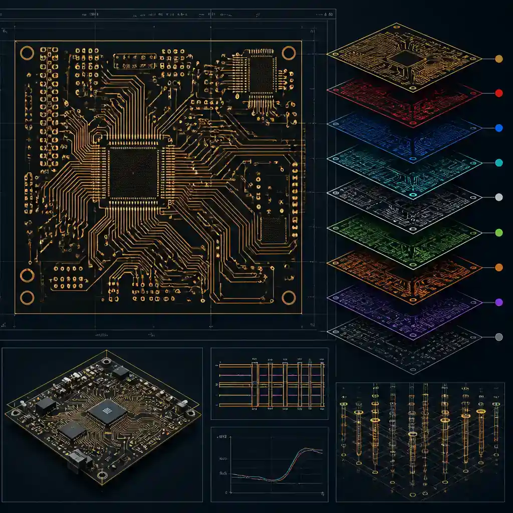
We accept Gerber RS-274X (.gbr, .gerber) and Excellon NC Drill (.drl, .txt) as the standard fabrication package. For PCBA, we also need BOM (.csv, .xlsx, .xls) and Pick & Place / CPL (.csv). We can work with ODB++ and IPC-2581 if available. Our CAM team handles conversion from all major EDA tools: Altium, Eagle, KiCad, OrCAD, Allegro, EasyEDA, Diptrace, PADS, and Proteus.
A complete BOM should include: designator (reference ID), MPN (manufacturer part number), quantity, description/package type, and preferred manufacturer. Optional but helpful: alternate MPNs (for sourcing flexibility), Digi-Key/Mouser part numbers, and any special notes (e.g., "do not substitute", "matched pair"). Our procurement team reviews the BOM and flags any availability issues before we quote.
Design for Manufacturability (DFM) review is our engineering team's pre-production analysis of your design files to identify potential manufacturing issues. We check: trace/space violations, annular ring adequacy, solder mask slivers, acid traps, copper-to-edge clearance, drill aspect ratios, and impedance stackup feasibility. A good DFM review catches issues that would cause fabrication defects, saving you time, cost, and re-spins. Our DFM review is free and included with every quote.
Yes. Our engineering team provides design guidance for new clients: we'll review your concept, recommend stackup configurations, suggest cost-optimized material choices, and advise on DFM best practices. We don't offer full PCB layout services, but we can connect you with trusted design partners. For startups and first-time PCB buyers, we recommend starting with a DFM tips review and sending us your files early, even rough drafts, for preliminary feedback.
Gerber files (RS-274X) are the industry-standard format for PCB fabrication data, one file per layer (copper, solder mask, silkscreen, board outline). Every EDA tool has a CAM processor or "Plot" function to export Gerbers. Typically: File → Plot / Fabrication Outputs → select layers → check "RS-274X" format → generate. We have a detailed guide in our Gerber files guide. If you're stuck, send us your EDA source files and we'll help with the export.
Yes. We sign Mutual NDAs (Non-Disclosure Agreements) as a standard practice before reviewing your design files. All client design data is stored on air-gapped internal servers, not cloud-connected. Access is restricted to the engineering team assigned to your project. We never share, reuse, or reverse-engineer client designs. See our Privacy Policy for full details on design file confidentiality.
Don't see your question here?

Our engineering team responds within 24 hours.