
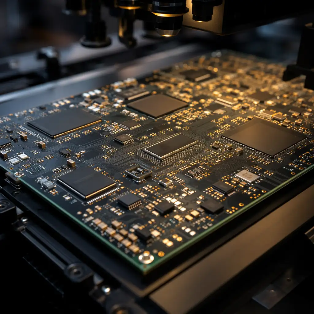
Capabilities / PCBA Assembly
8 high-speed SMT lines running 24/6. 01005 passives through BGA/QFN. IPC-A-610 Class 2/3. IATF 16949 & ISO 13485 certified. Free assembly DFM review. We validate your BOM, placement, and paste stencil before the first component is placed.
Core Specifications
From 01005 (0.4×0.2mm) chip components to large BGAs (>55mm), QFNs, CSPs, LGAs, and PoP (Package-on-Package). Fine-pitch down to 0.25mm BGA and 0.3mm QFP. Connectors, relays, transformers, and shielded modules.
High-speed modular SMT lines with dual-lane capability. Up to 200,000 components per hour per line. Automatic changeover reduces downtime between batches. Suitable for both high-mix low-volume and mass production runs.
Standard PCB size up to 510×460mm. Extended rail up to 1,200×510mm for LED strips and backplanes. Board thickness 0.3mm–6.0mm. Panel up to 600×800mm with fixture support for over-sized assemblies.
SMT reflow, 10-zone oven, N₂ atmosphere, ±1.5°C profile control. Wave soldering . Dual-wave for mixed-technology boards. Selective soldering . Nozzle-based for through-hole on double-sided SMT. Lead-free (SAC305) or leaded (Sn63Pb37).
IPC-A-610 Class 2 as standard for commercial/industrial products. Class 3 for aerospace, medical, and automotive. IPC J-STD-001 for soldering process. ANSI/ESD S20.20 ESD control.
Every order includes a free assembly DFM review. We validate footprint-to-package match, paste stencil aperture, polarity/orientation, component spacing, and BOM part number cross-reference before production start.
Laser-cut stencil (0.08–0.2mm). Automatic paste inspection (SPI). 100% area coverage check per pad.
High-speed & fine-pitch placement. Vision alignment. Real-time component verification. Feeder and reel traceability.
10-zone profile. N₂ atmosphere. ±1.5°C per zone. Ramp-soak-spike to J-STD-020. Post-reflow cooling control.
3D AOI on every board after reflow. Solder joint quality, bridging, tombstoning, lifted leads. Automatic pass/fail.
ICT, FCT, flying probe. X-Ray for BGA/QFN. Conformal coating. Final QA before packaging.
| Parameter | Standard | Advanced |
|---|---|---|
| SMT Lines | 8 high-speed lines | Dedicated NPI line for prototypes |
| Placement Speed | Up to 200,000 CPH / line | Dual-lane, concurrent placement |
| Smallest Component | 0201 (0.6×0.3mm) | 01005 (0.4×0.2mm) |
| Largest Component | 55×55mm BGA | On request |
| Fine-Pitch BGA | 0.25mm pitch minimum | |
| Fine-Pitch QFP/QFN | 0.3mm pitch minimum | |
| Board Size | 50×50mm–510×460mm | Up to 1,200×510mm (extended rail) |
| Board Thickness | 0.8mm–3.2mm | 0.3mm–6.0mm |
| Solder Type | SAC305 (Pb-free), Sn63Pb37 (leaded) | |
| Stencil Thickness | 0.1–0.15mm laser-cut SS | 0.08–0.2mm, stepped stencils |
| Reflow Zones | 10-zone, N₂ atmosphere | |
| Wave Soldering | Dual-wave, lead-free | |
| Selective Soldering | Nozzle-based, programmed per board | |
| Conformal Coating | Acrylic, silicone, polyurethane. Selective spray + manual touch-up | |
| Potting / Encapsulation | Epoxy, silicone, polyurethane. Vacuum degas available. | |
| Workmanship | IPC-A-610 Class 2 | IPC-A-610 Class 3 / J-STD-001 Space |
| ESD Control | ANSI/ESD S20.20, full ESD flooring & grounding | |
Solder Paste Inspection on every print. 3D volumetric measurement. 100% pad coverage. Catch stencil issues before placement, no rework downstream.
Automatic Optical Inspection on every board after reflow. 3D solder joint profiling. Bridging, tombstoning, lifted leads, missing components. Automatic pass/fail with human review on borderline cases.
2D/3D X-Ray for BGA, QFN, and hidden joints. Void detection, solder ball integrity, bridging under packages. Mandatory for Class 3 assemblies. Programmable inspection paths per board design.
In-Circuit Test, bed-of-nails fixture per design. Component value verification, open/short detection, polarity check. Fixture design and fabrication in-house. Flying probe available for low-volume / prototype.
Functional Circuit Test, powered-on board exercising real operating conditions. Custom test jig per product. Firmware flashing, calibration, and burn-in available. Full test report with every shipment.
Cross-section analysis for process validation and failure analysis. Microscope to 500×. Solder joint IMC layer verification. Included with NPI runs. On-demand for production QA sampling.
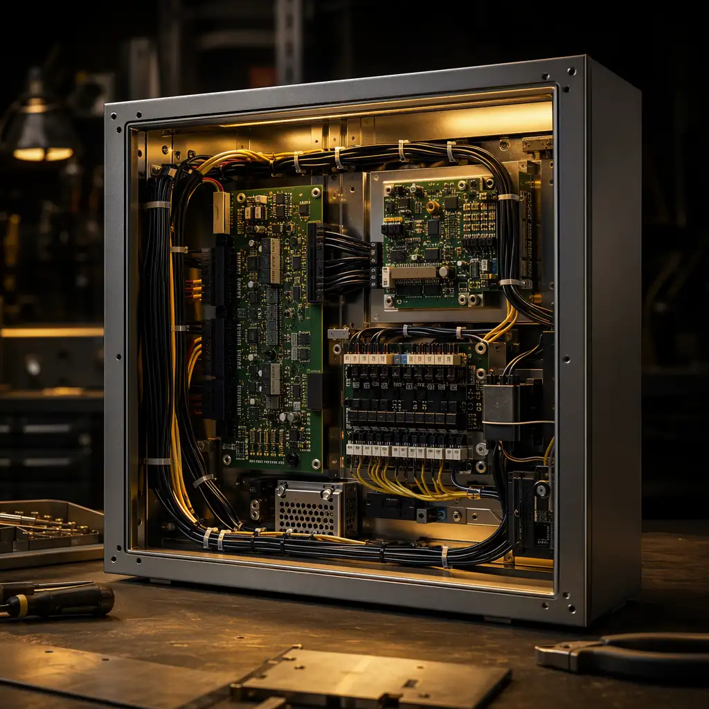
Box-Build Integration
Assembly doesn't stop at the board. Our box-build service integrates PCBA into enclosures, cable harnesses, and finished products, tested, labeled, and retail-ready. We manage the full assembly chain, so you receive a product that's ready to ship to your customer or warehouse.
General-purpose. Good moisture & fungus resistance. Easy rework. Widely used in consumer, industrial, and IoT products.
Wide temperature range (-65 to +200°C). Excellent for automotive under-hood and aerospace high-temp environments.
Excellent chemical & abrasion resistance. Fuel and solvent resistant. Common in industrial and harsh environments.
Vapor-deposited nano-coating. Ultrathin (0.1–25µm), pinhole-free. The gold standard for medical implants and mil/aero electronics.
| Station | Equipment | Capability |
|---|---|---|
| Solder Paste Printer | DEK Horizon 03iX / EKRA X5 | ±12.5µm alignment @ 2 Cpk. 2D + 3D SPI integration. Automatic stencil cleaning. |
| High-Speed Placer | Yamaha YSM40R / ASM SIPLACE TX2 | Chip shooter: 01005–1005 at 200K CPH. 8× vision alignment. Dual-lane parallel placement. |
| Fine-Pitch Placer | Yamaha YSM20WR / ASM SIPLACE SX2 | IC placer: BGA, QFP, QFN, CSP. 0.25mm BGA pitch. POP capable. ±15µm placement accuracy. |
| Reflow Oven | Heller 1913 Mk5 / ERSA Hotflow 3/20 | 10 zones, N₂ atmosphere. ±1.5°C ΔT. Dual-lane capable. Vacuum soldering option for void reduction. |
| AOI | Koh Young Zenith 2 / Mirtec MV-6 | 3D AOI with AI classification. 100% coverage in 4 angles. 25µm resolution. Real-time SPC. |
| X-Ray | Nikon XT V 160 / Nordson Dage Quadra 5 | 2D/3D X-Ray. Automatic void analysis. BGA/QFN/LGA inspection. 0.5µm feature detection. |
| Conformal Coating | Nordson Asymtek Select Coat SC-350 | Selective spray + needle dispense. Programmable per-board. UV-cure option. |
Upload your BOM (Excel or CSV), Gerber files, and assembly drawing. We'll return a full DFM report, component availability check, footprint validation, and placement feasibility, all within 24 hours.

Upload BOM and Gerber files. Free review in 24 hours.