
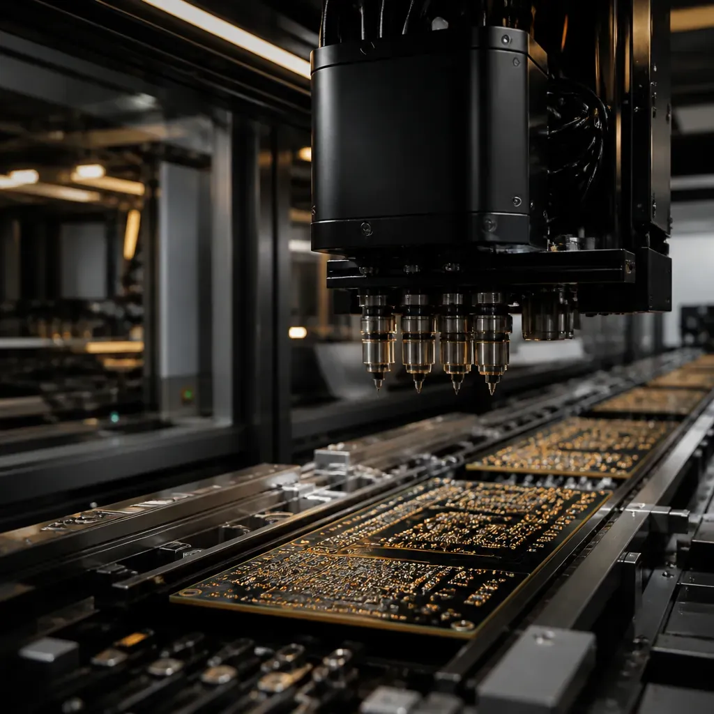
Your Manufacturing Journey
From Gerber upload to global delivery, a transparent, 7-step process designed for busy engineers and procurement teams.
7-Step Process
Every step is monitored. You receive updates at each milestone, no black boxes, no surprises.
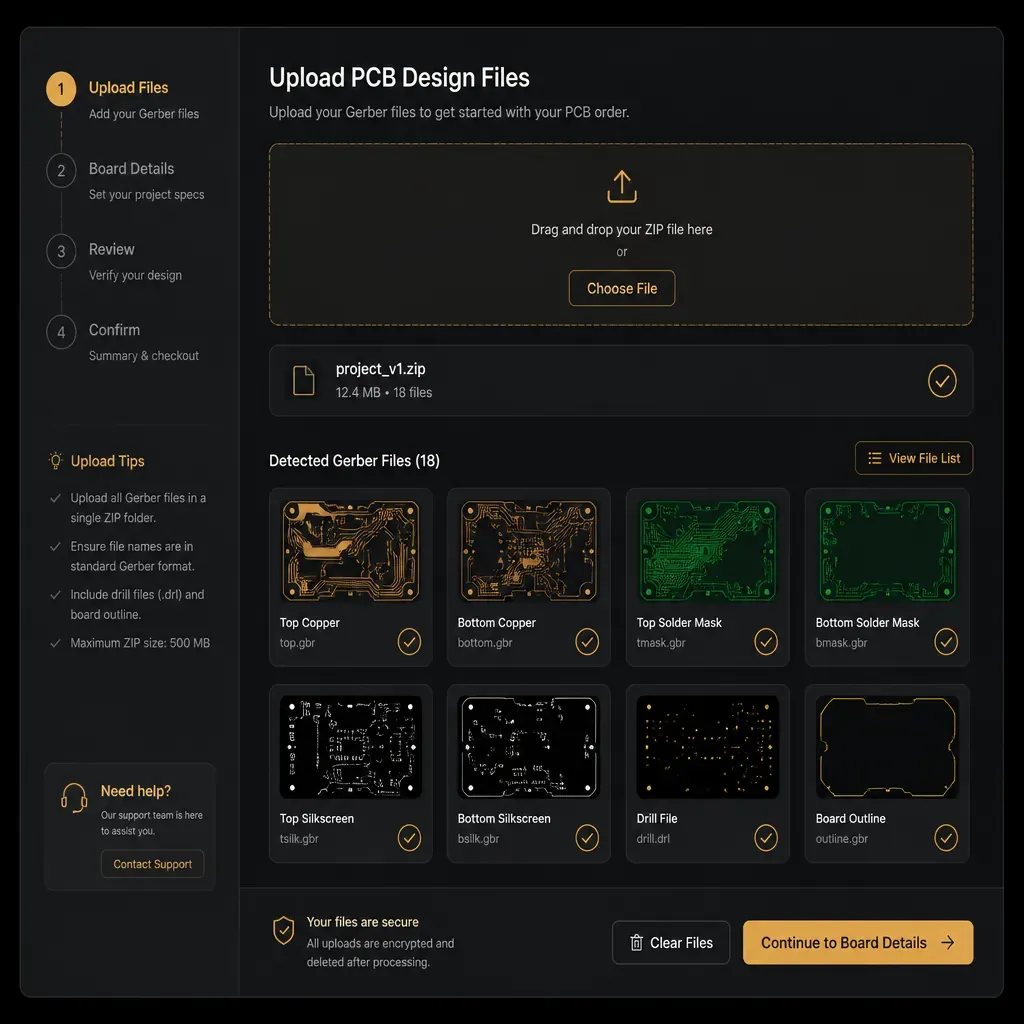
Send us your Gerber files (RS-274X), drill files, and BOM if you need PCBA. For PCB-only orders, Gerber + drill is all we need. We accept Eagle, Altium, KiCad, OrCAD, and all major EDA formats, our CAM team handles the conversion.
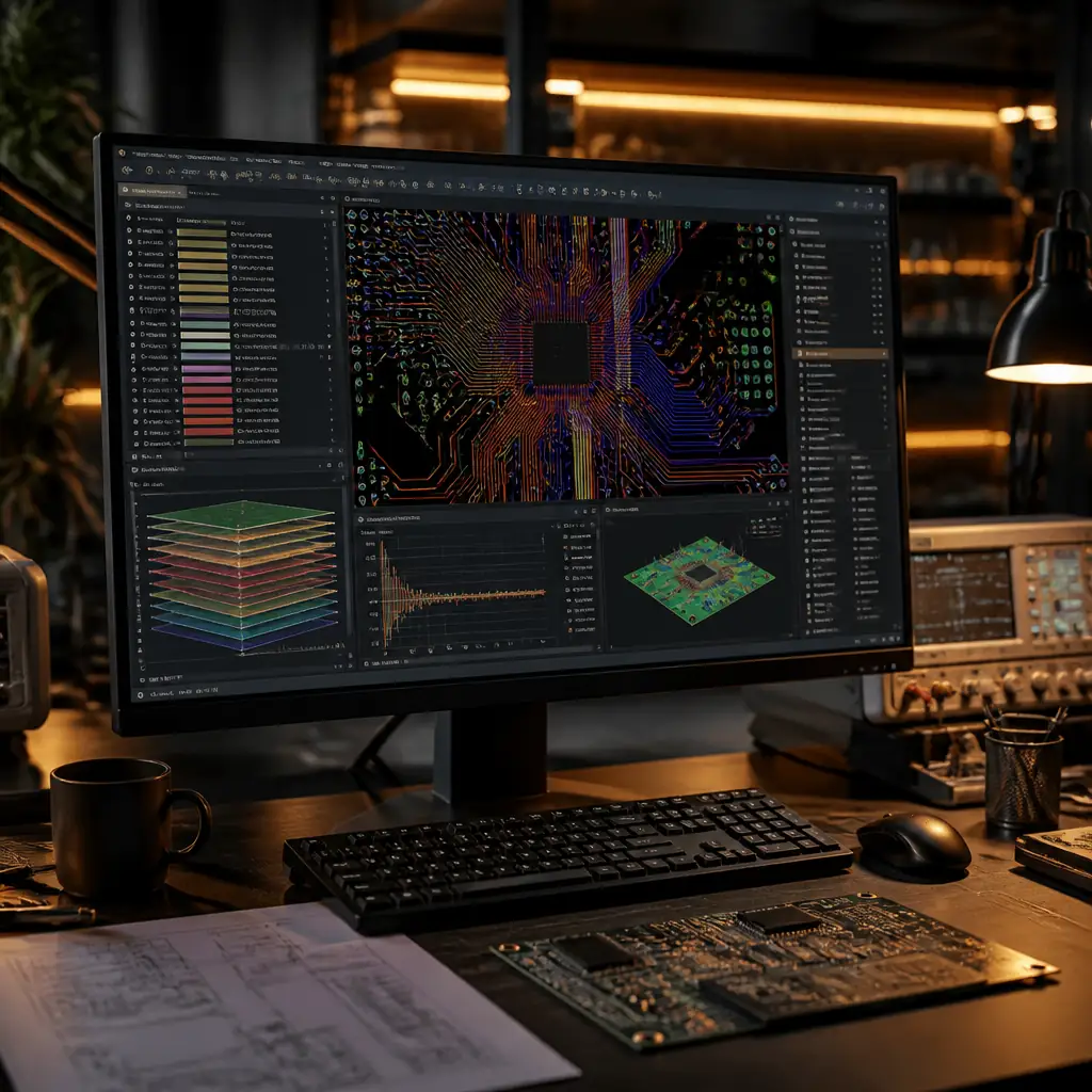
Within 4 business hours, our CAM engineers run a comprehensive Design for Manufacturability check. We verify trace/space, annular rings, solder mask clearances, drill-to-copper distances, and impedance stackup feasibility, against your target IPC class.
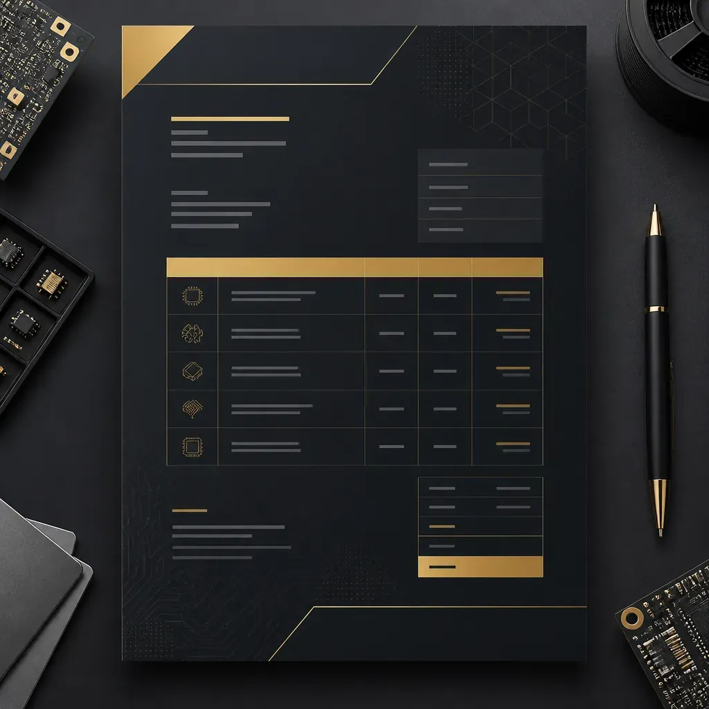
You receive a detailed quotation with unit price breakdown, NRE costs, tooling fees, and shipping estimates, all itemized. No hidden charges. Once approved, we issue a Proforma Invoice. Production begins upon PO confirmation. For new clients, we recommend starting with a prototype batch to validate quality before scaling.
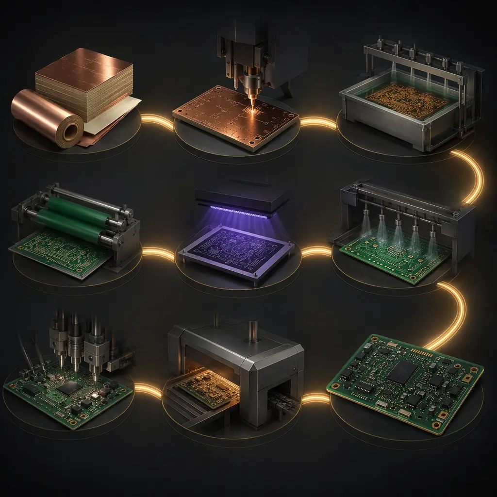
Your boards enter our 80,000㎡ facility. The process includes: inner layer imaging & etching → AOI inspection → lamination → drilling → electroless copper deposition → outer layer imaging → pattern plating → etching → solder mask application → surface finish → silkscreen → electrical test → final inspection.
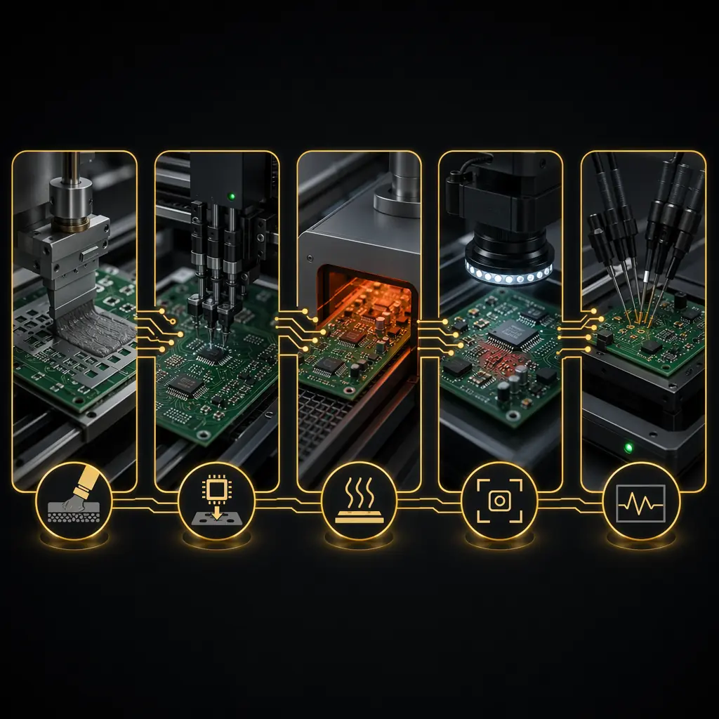
If your order includes assembly: we source components from 50+ authorized distributors (Digi-Key, Mouser, Arrow, Avnet, LCSC) or use your consigned parts. Our 8 high-speed SMT lines handle 0201 to 55mm BGA. 3D SPI before reflow, 10-zone reflow ovens, inline AOI after each side, and X-Ray for BGA/QFN verification.

Every board passes through our multi-stage QC gate: visual inspection → AOI → electrical test (100% netlist) → microsection analysis (batch sample) → solderability test → ionic contamination test → dimensional verification. PCBA orders add: first-article inspection, ICT/flying probe, functional test per your spec, burn-in testing if required.

Boards are vacuum-sealed with desiccant and humidity indicator cards, packed in anti-static foam-lined cartons. We ship via DHL, FedEx, UPS, TNT (3–5 days express) or sea/rail freight for volume orders. Every shipment includes: QC inspection report, Certificate of Conformance, RoHS/REACH compliance docs, and traceability records.
File Requirements
Most EDA tools export these directly. If you're unsure, our engineers will guide you, just reach out.
RS-274X format. One file per layer (copper, mask, silkscreen, outline). Generated from your EDA tool's CAM processor.
Excellon format. Contains all drill hole positions, sizes, and plating flags. Required for all PCB orders.
For PCBA orders. Part numbers, quantities, designators, and preferred manufacturers. CSV or Excel format.
Supported EDA tools: Altium Designer, Eagle, KiCad, OrCAD, Allegro, EasyEDA, Diptrace, PADS, Proteus, and any tool that exports standard Gerber.
Quality Commitment
We don't sample-test: every single board passes through AOI and electrical test. Our IPC Class 3 production line is audited quarterly. If any board fails our outgoing inspection, the entire batch is reworked or remanufactured at our cost.
Upload your Gerber files now. Free DFM review, 24-hour quote, 5-7 day production. No registration, no commitment.

Upload Gerber + BOM, 24h quote with free DFM review.