
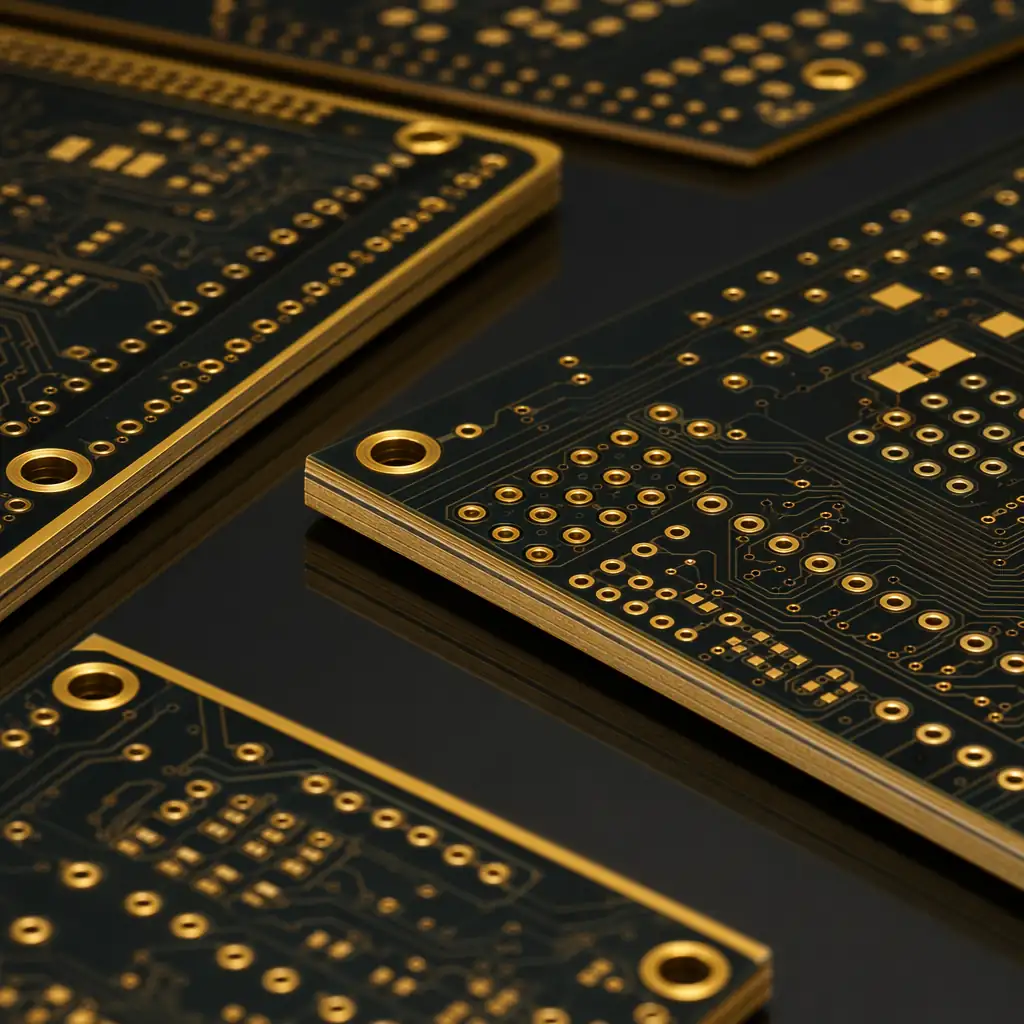
Capabilities / PCB Fabrication
2–32 layers. Any-layer HDI. 3/3mil trace/space. Rogers, PTFE, ceramic, aluminum, polyimide. 100% AOI + flying probe E-test on every board. IATF 16949 & UL certified. Free DFM review on every order.
Core Specifications
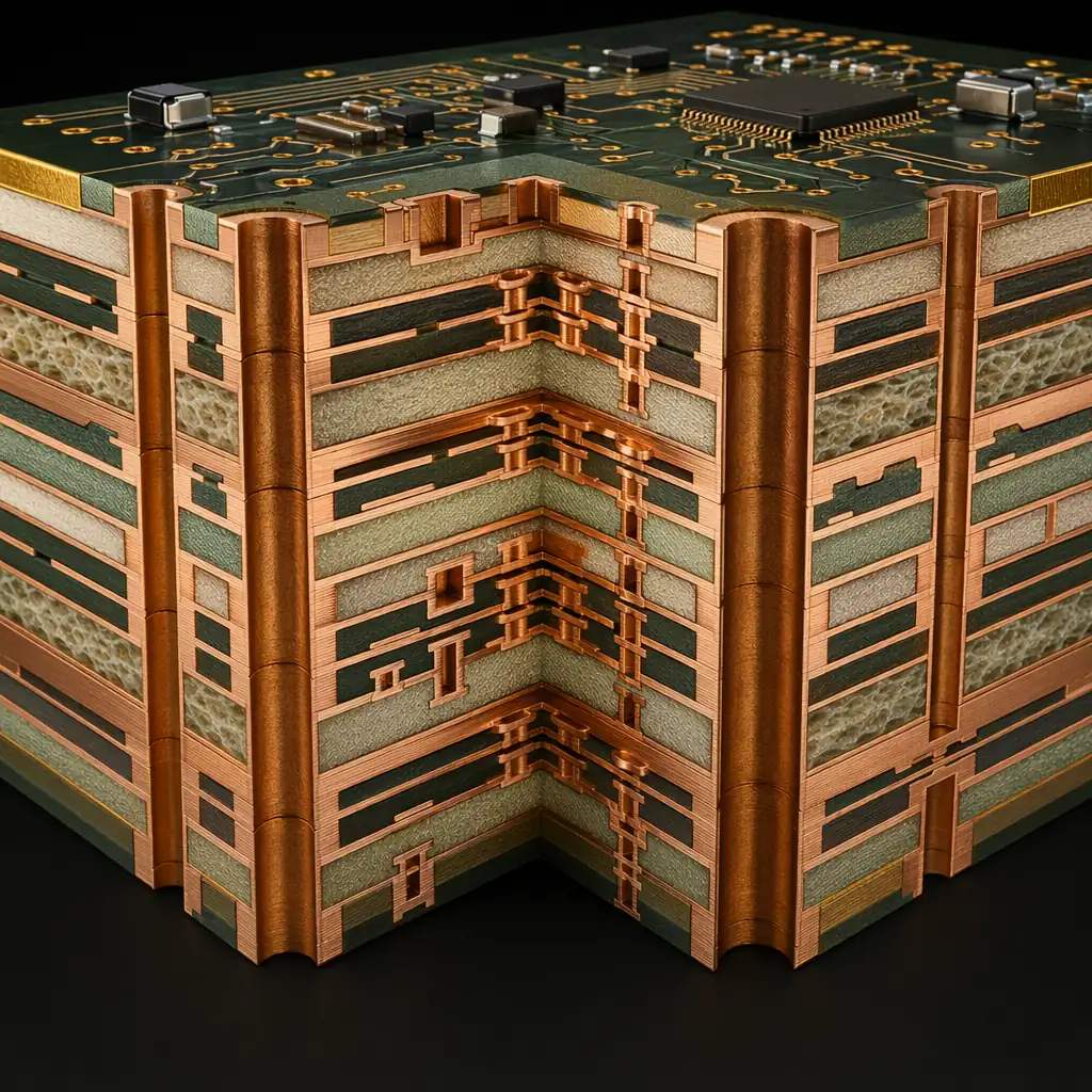
Standard 2–16 layers with 5-day production. Advanced 18–32 layers with blind/buried vias, back-drill, and any-layer microvia stacking. Up to 60 layers available on request for complex backplanes.
Standard 5/5mil for cost-optimized production. Advanced 3/3mil for high-density designs. Laser-drilled microvias down to 75µm (0.075mm). Min annular ring 0.15mm. Aspect ratio up to 16:1.
Standard panels up to 500×600mm. Large-format up to 600×800mm for backplanes and industrial applications. Thickness range 0.2mm–6.0mm with ±10% tolerance for boards ≥1.0mm.
Standard inner layers 1–4oz, outer 1–8oz. Heavy copper up to 12oz for high-current power electronics, BMS, and motor drives. Thick copper ground planes for thermal management.
TDR-verified on every controlled-impedance panel. Standard ±10%, advanced ±5%. Critical for 5G/telecom, high-speed digital (PCIe Gen5, 100GBASE-KR4), and RF applications.
100% flying probe or fixture E-test on every board. 100% AOI. IPC-A-600 Class 2 as standard, Class 3/3A for aerospace, automotive, and medical. X-Ray on multilayer registration.
HDI Technology
HDI (High-Density Interconnect) technology enables the compact, high-performance PCBs required by modern electronics, from smartphone mainboards to ADAS controllers. Our any-layer HDI process uses laser-drilled microvias to connect any layer to any other layer, maximizing routing density and signal integrity.
| Parameter | Standard | Advanced |
|---|---|---|
| Layer Count | 2–16 layers | 18–32 layers (up to 60 on request) |
| Board Thickness | 0.4mm–3.2mm | 0.2mm–6.0mm |
| Thickness Tolerance | ±10% (≥1.0mm) | ±0.1mm (<1.0mm) |
| Min Trace / Space | 5/5mil (0.127mm) | 3/3mil (0.076mm) |
| Min Mechanical Hole | 0.25mm | 0.15mm |
| Min Laser Via | 0.10mm | 0.075mm |
| Max Mechanical Hole | 6.3mm | |
| Finished Hole Tolerance | ±0.08mm (PTH), ±0.05mm (NPTH) | |
| Min Annular Ring | 0.15mm (6mil) | |
| Aspect Ratio | Up to 16:1 | |
| Max Board Size | 500×600mm | 600×800mm |
| Min Board Size | 5×5mm | |
| Inner Copper Weight | 1–4oz | Up to 6oz |
| Outer Copper Weight | 1–8oz | Up to 12oz |
| Impedance Control | ±10% | ±5% (TDR verified) |
| HDI Type | 1+N+1, 2+N+2 | Any-Layer (stacked µvias) |
| Min Plated Half-Hole | 0.5mm | |
| Bow & Twist | ≤0.75% | ≤0.5% |
| Material | Tg / Key Property | Typical Applications | Availability |
|---|---|---|---|
| FR-4 (Standard) | Tg 130–140°C | Consumer electronics, general-purpose | In stock |
| High-Tg FR-4 | Tg 170–180°C | Automotive, industrial, lead-free assembly | In stock |
| Rogers 4350B / 4003C | Dk 3.48 / 3.38, Df 0.0037 / 0.0027 | 5G base stations, radar, satellite RF | In stock |
| PTFE (Taconic / Arlon) | Dk 2.1–2.9, ultra-low Df | mmWave, aerospace radar, satellite transceivers | 2–5 day lead |
| Aluminum (Metal-Core) | Thermal cond. 1.0–3.0 W/m·K | LED lighting, power supplies, motor drives | In stock |
| Ceramic (Al₂O₃ / AlN) | Thermal cond. 20–170 W/m·K | Aerospace RF, high-power amplifiers, T/R modules | 3–7 day lead |
| Polyimide | Tg 250°C+ | Flex/rigid-flex, aerospace, medical implants, downhole | 2–5 day lead |
| Mixed / Hybrid Laminates | FR-4 + Rogers/PTFE stack-up | Cost-optimized RF/digital mixed-signal boards | On request |
| Finish | Thickness | Best For | Shelf Life |
|---|---|---|---|
| ENIG (Immersion Gold) | Ni 3–6µm, Au 0.05–0.15µm | Fine-pitch BGA, consumer, general purpose | 12 months |
| ENEPIG | Ni 3–6µm, Pd 0.05–0.15µm, Au 0.05–0.1µm | Wire bonding, press-fit, high-reliability | 12 months |
| HASL (Lead-Free) | 1–40µm | Through-hole, general purpose, cost-sensitive | 12 months |
| Immersion Silver | 0.15–0.5µm | High-frequency RF, smooth surface | 6–12 months |
| Immersion Tin | 0.8–1.2µm | Press-fit connectors, fine-pitch | 6 months |
| OSP (Organic) | 0.2–0.5µm | Cost-sensitive, short shelf-life projects | 6 months |
| Hard Gold | Ni 3–6µm, Au 0.5–1.5µm (30–50µ") | Edge connectors, keypads, high-cycle interfaces | 24 months |
Remove unused via stubs for >5Gbps signal integrity. Controlled depth ±50µm. Burr-free. Typical for high-speed backplanes and telecom line cards.
Wrap-around copper on board edges for EMI shielding, grounding, and thermal conduction. Common in aerospace enclosures and RF modules.
Hard gold (30µ" or 50µ") on nickel underplate. Beveled edges (20°/30°/45°). For PCIe cards, memory modules, and line-replaceable units.
Precision depth-controlled drilling for flush-mount screws and connector housings. ±0.1mm depth tolerance. Multi-depth on same board.
Carbon ink for keypad contacts and jumpers. Peelable solder mask for selective wave-solder masking. Both applied by screen printing.
Copper-filled and planarized vias directly in SMD pads. Essential for 0.4mm and below BGA pitch. Flatness verified by optical profilometer.
| Option | Available Colors / Types |
|---|---|
| Solder Mask | Green, Blue, Black, White, Red, Yellow, Matte Green, Matte Black, Purple, Transparent |
| Silkscreen / Legend | White, Black, Yellow |
| Solder Mask Type | LPI (Liquid Photo-Imageable), standard for all colors |
| Min Solder Mask Dam | 0.1mm (4mil), standard; 0.075mm (3mil), advanced |
| Min Silkscreen Line Width | 0.15mm (6mil) |
Upload your design files, Gerber, drill, stackup, and any special requirements. Our engineering team will respond within 24 hours with a detailed DFM analysis and quote. No commitment required.

Upload Gerber files and specs. Free DFM review within 24 hours.