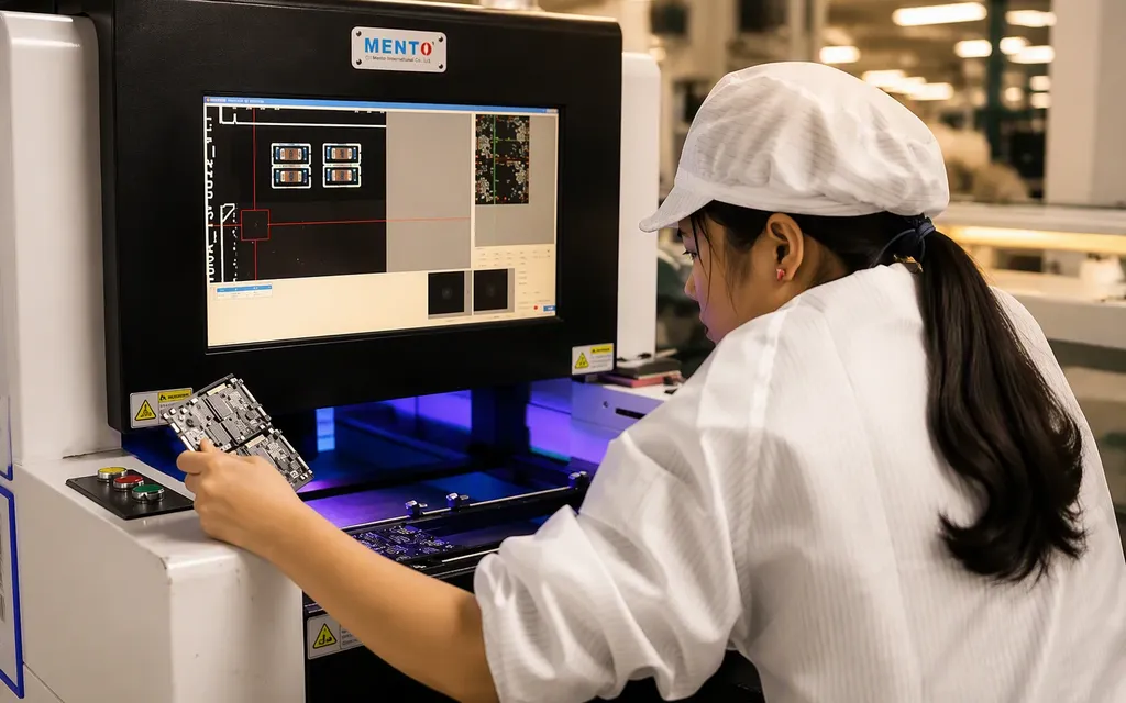
Trust Through Testing
IPC-A-610 Class 2 and Class 3. 100% inspection. Seven-stage QC process. ISO 9001 & UL certified for automotive-grade reliability.
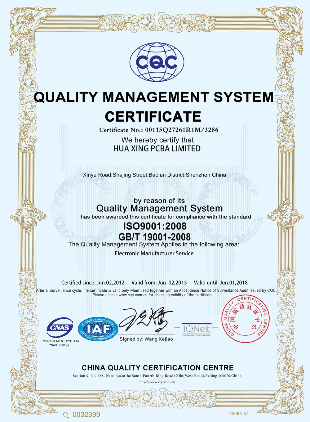
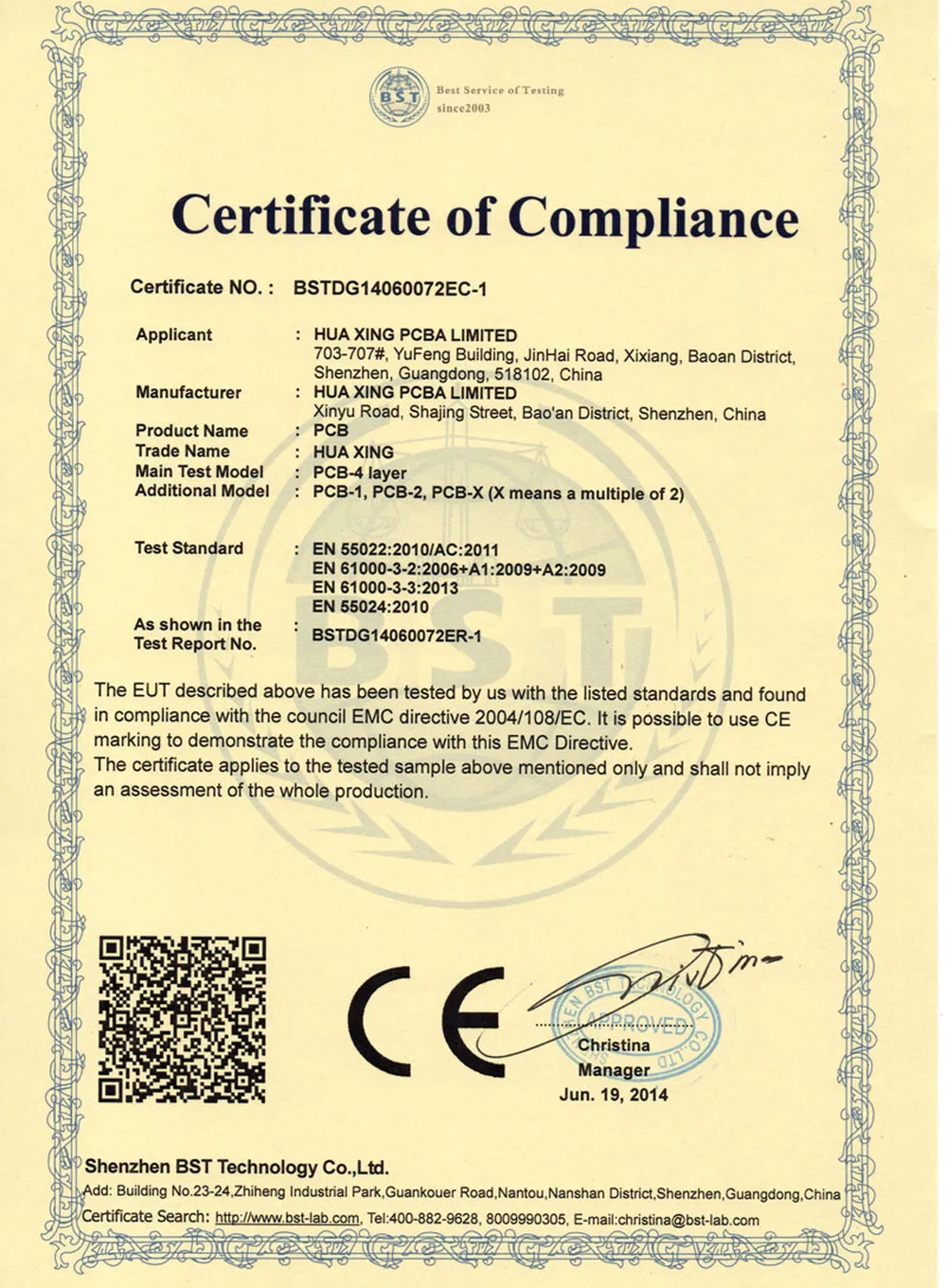
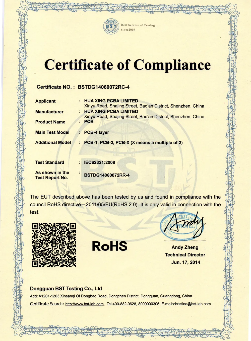
Certifications

Safety certification for PCB materials and finished boards. UL file available.

Restriction of hazardous substances. REACH compliant processes, certificate on file.

EMC directive compliance per EN 55022 / EN 61000 series. Scan available on request.

China Quality Certification. Factory audited and product certified.

IPC-A-610 Class 2 & 3 acceptance. IPC-9252 electrical test. IPC-1601 handling.
Quality Control Process
Incoming material inspection: laminates, solder mask, chemicals, components, verified against spec before production
3D solder paste inspection on every SMT line before reflow, paste volume, height, area and offset measured in real time
100% automated optical inspection: opens, shorts, trace width violations, solder mask defects, both sides scanned
2D and CT X-Ray for BGA, QFN and hidden joints. Void analysis per IPC-7095. Standard on every BGA/QFN assembly
100% electrical test, flying probe for prototype/NPI, bed-of-nails ICT at volume. IPC-9252 Class 2 compliance
In-circuit and functional test with golden-sample verification: power-up, communication protocols, sensor calibration
Final visual + outgoing quality check. Vacuum-sealed packaging per IPC-1601. Documentation pack assembled
Testing Capabilities
2D and 3D AOI systems from Koh Young and Omron. Detects solder bridges, tombstoning, missing components, lifted leads, and polarity errors at production speed. 100% coverage, both sides, every board.
2D and CT X-Ray for BGA, QFN, and hidden-joint inspection. Void analysis per IPC-7095. Detects head-in-pillow, insufficient solder, and pad cratering. Standard on all BGA and QFN assemblies.
Flying probe for prototype and NPI (no fixture cost). Bed-of-nails ICT for volume production. Tests: opens, shorts, component values, diode/transistor orientation, capacitance, inductance. IPC-9252 compliant.
TDR (Time Domain Reflectometry) impedance testing with ±5% tolerance guarantee. Test coupons on every controlled-impedance panel. Polar Instruments CITS880s system. Report included with shipment.
Custom functional test fixtures built to your specification. Simulates real operating conditions: power-up, signal integrity, communication protocols, sensor calibration. Golden-sample verification before every run.
Destructive analysis on sacrificial coupons per production batch. Measures: copper plating thickness, intermetallic layer formation, hole wall quality, dielectric thickness, solder mask registration. Per IPC-6012.
Koh Young 3D SPI on every SMT line, before reflow. Measures paste volume, height, area, and offset. Catches insufficient paste, bridging, and misalignment before it becomes a defect. Real-time SPC feedback loop.
Solderability testing per IPC-J-STD-003 on test coupons. Thermal stress testing (288°C / 10s float) for delamination resistance. Tin whisker mitigation verification for lead-free finishes.
Automated UV inspection of conformal coating coverage and thickness per IPC-CC-830. Black-light booth for manual verification on complex geometries. Coating thickness measured at 5-point grid per board.
| Requirement | IPC Class 2 (Industrial) | IPC Class 3 (High Reliability) |
|---|---|---|
| Annular Ring (External) | 90° breakout allowed | Min. 0.05mm annular ring, no breakout |
| Annular Ring (Internal) | 90° breakout allowed, not connected | Min. 0.025mm annular ring |
| Solder Joint (PTH) | 180° circumferential wetting | 270° minimum, 330° preferred |
| Plating Void | < 5% of barrel length | < 2.5% of barrel length |
| Etchback / Negative Etchback | Allowed if no resin smear | Not permitted, positive etchback required |
| Solder Mask Clearance | ±0.075mm registration | ±0.05mm registration |
| Dielectric Spacing | > 0.09mm (external) | > 0.13mm (external) |
| Typical Applications | Industrial, consumer, commercial | Automotive, medical, aerospace, defense |
| Inspection Level | Sampling + 100% AOI/E-test | 100% visual + AOI + E-test + microsection |
| Cost Premium vs Class 2 | , | ~20–30% |
Continuous Improvement
Every critical process parameter, plating thickness, etch factor, line width, registration accuracy, solder paste volume, is monitored in real time via Statistical Process Control (SPC). Control charts track Cp and Cpk indices, triggering automatic alerts when any parameter drifts beyond ±1.5σ.
Each production batch includes a complete QC documentation package: AOI images, electrical test reports (IPC-9252), impedance test data (TDR plots), microsection images with measurements, Certificate of Conformance, RoHS/REACH compliance, and lot traceability records, archived for 3 years.
If any board fails outgoing QC inspection, we perform a root cause analysis and either rework or remanufacture, at our cost. For IPC Class 3 orders, any non-conformance triggers a full batch review, a corrective action report (CAR), and preventive action implementation within 48 hours. Your design files, production parameters, and test fixtures are retained for consistent quality across re-orders.
Request our quality manual, certificates, or a sample QC documentation package. See how we ensure zero-defect delivery.

Upload Gerber + BOM, 24h quote with free DFM review.