
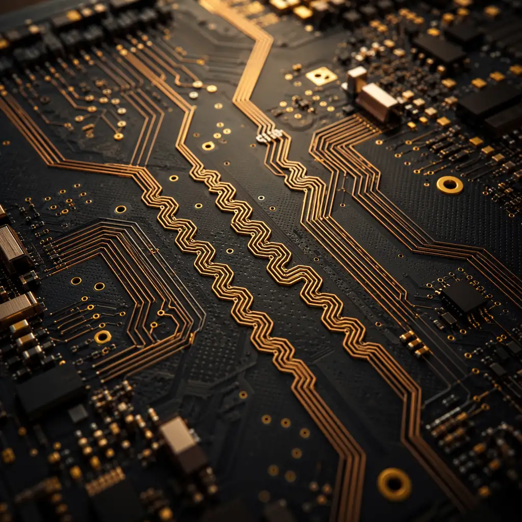
PCB Types / High-Speed Digital PCB
As data rates push beyond 56Gbps PAM4 toward 112Gbps and 224Gbps, PCB materials and geometries become the limiting factor. Our high-speed digital capability pairs ultra-low-loss Megtron 6/Tachyon-100G laminates with back-drilling, HVLP copper, and precision impedance control, qualified for 800G data center and 5G infrastructure.
Technology Overview
At 56Gbps PAM4 and above, every discontinuity in the signal path, via stubs, copper roughness, glass-weave skew, impedance variations, degrades the eye diagram and increases bit error rate. High-speed digital PCB design is an exercise in managing these loss mechanisms through material selection, geometry control, and precision manufacturing.
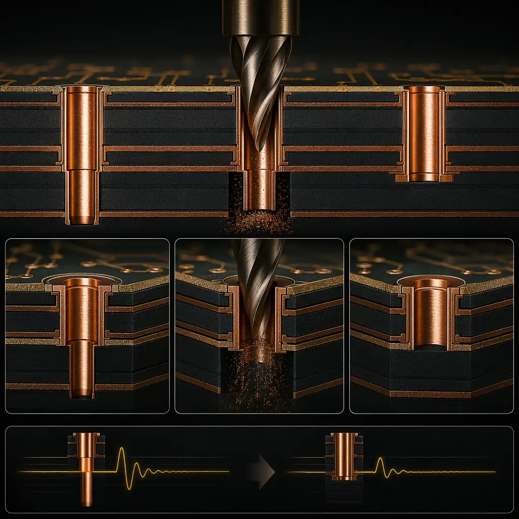
The three pillars of high-speed PCB manufacturing are: (1) ultra-low-loss laminates with tight Dk/Df control, (2) ultra-smooth copper to reduce conductor loss from skin effect, and (3) back-drilling to remove via stubs that cause destructive resonant nulls. We combine all three with TDR-verified impedance control on every panel.
Technical Specifications
| Laminate Portfolio | Megtron 6/7/8 · Tachyon-100G · I-Tera MT40 · RO4835 · N4000-13 EP/EP SI · EM-888/EM-891 |
| Max Data Rate | 112 Gbps PAM4 (56 Gbaud); 224Gbps on evaluation |
| Dielectric Constant (Dk) | 3.02 – 3.70 across laminate portfolio |
| Dissipation Factor (Df) | As low as 0.0017 @10GHz (Tachyon-100G) |
| Number of Layers | 8 – 40+ layers; 40+L requires evaluation |
| Copper Foil | HVLP (Rz ≤1.5µm) · VLP (Rz ≤3.0µm) · RTF for non-critical layers |
| Min. Trace / Space | 3 / 3 mil (0.075 / 0.075 mm) on smooth copper |
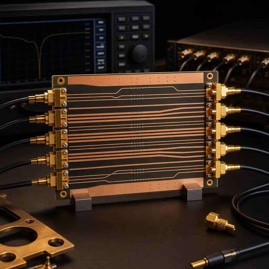
| Impedance Control | ±5% single-ended; ±7% differential; TDR report on every panel |
| Intra-Pair Skew | ≤ ±1 ps on differential pairs (glass-weave mitigation) |
| Back-Drill | Stub removal ≤10 mil; depth tolerance ±2 mil; 100% depth-checked |
| Surface Finish | ENIG · ENEPIG · Immersion Ag · OSP |
| Quality Standard | IPC-6012 Class 3 · IATF 16949 · ISO 9001 |
Industry-standard ultra-low-loss laminate for 28-56Gbps designs. Excellent processability. Available in wide range of glass styles and resin contents. Most cost-effective entry point for high-speed digital.
Lowest-loss FR-4 compatible laminate for 112Gbps PAM4. Extremely low Dk for reduced propagation delay. Spread-glass reinforcement for superior CAF resistance and laser via compatibility.
Mid-loss option for cost-sensitive 10-25Gbps designs. Good thermal reliability at lower price point than Megtron 6. Used extensively in telecom line cards and enterprise servers.
Nelco low-loss laminate with enhanced signal integrity. Competitive alternative to Megtron for 10-28Gbps range. Good laser via performance for HDI + high-speed hybrid designs.
Manufacturing Process
Via stubs, the unused portion of a plated through-hole beyond the last connected layer, create an unterminated transmission line stub that causes destructive reflections at high frequencies. Back-drilling removes these stubs with a controlled-depth drill from the opposite side of the board, reducing the stub to a controlled length ≤10 mil.
800G switch backplane, NIC card, server motherboard
Baseband unit, fronthaul gateway, edge compute
GPU/TPU carrier, HBM interposer, PCIe 6.0 add-in card
Supercomputer node, FPGA prototyping, CXL memory
12G-SDI router, 8K video processor, HDMI 2.1 matrix
NVMe-oF controller, SAS 4.0 backplane, PCIe 5.0 SSD
Upload your high-speed design, we'll review stackup, material selection, back-drill requirements, and impedance targets. Free SI-focused DFM report within 24 hours.

Tell us data rate, preferred laminate, layer count, back-drill needs. Free DFM within 24h.