
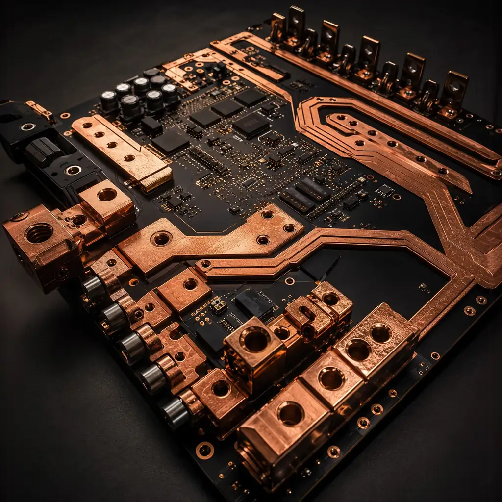
PCB Types / Heavy Copper PCB
Heavy copper PCBs carry high current and dissipate heat where standard boards fail. From 4oz to 12oz on outer layers, and custom bus bar constructions to 40oz, our heavy copper capability serves EV battery management, industrial welding, solar inverters, and high-current power distribution.
Technology Overview
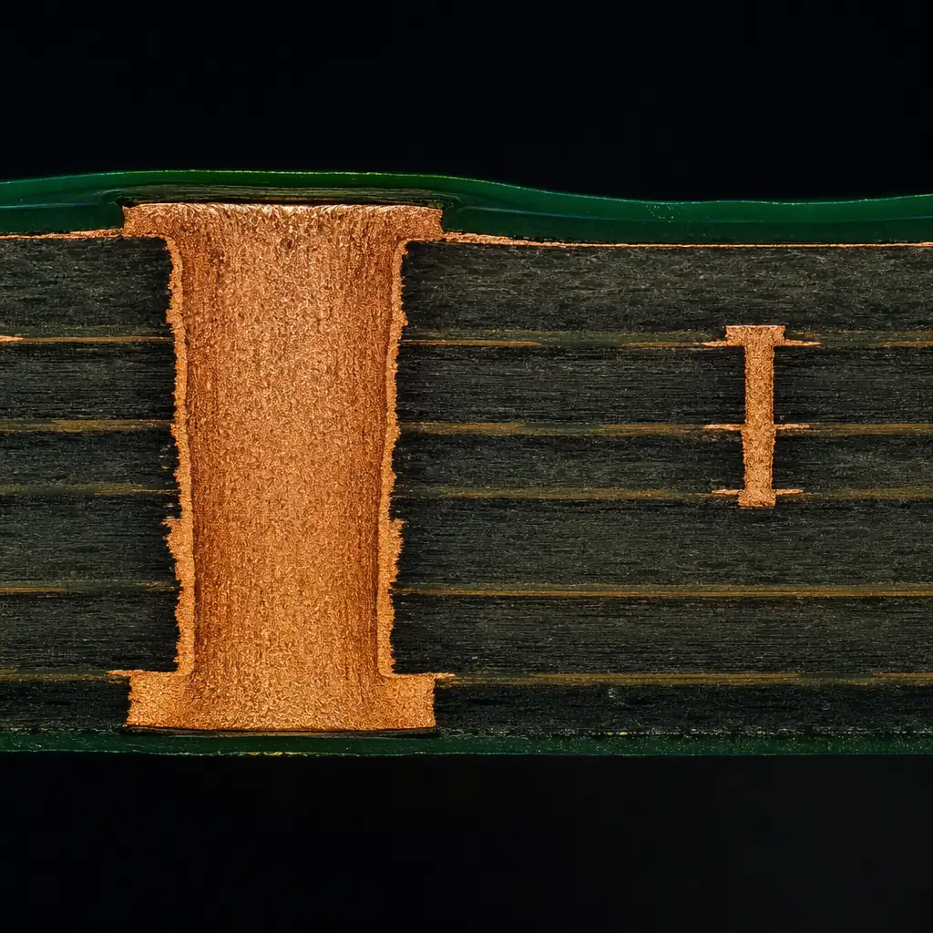
Standard PCBs use 1oz (35µm) copper, fine for signals, but insufficient for power electronics where currents reach tens or hundreds of amps. Heavy copper PCBs use copper thicknesses from 4oz (140µm) to 12oz (420µm) on outer layers, dramatically increasing current-carrying capacity and thermal dissipation.
The challenge isn't just plating thicker copper, it's etching fine features in thick foil, applying solder mask that won't crack over tall copper steps, and managing thermal expansion mismatches. Our heavy copper process addresses all three, with double-coat solder mask for copper weights above 4oz and controlled etch compensation for trace geometry integrity.
Technical Specifications
| Outer Copper Weight | 4 OZ – 12 OZ (140 – 420µm); 12oz as standard max |
| Inner Copper Weight | 1 OZ – 6 OZ (35 – 210µm); mixed weights supported |
| Number of Layers | 2 – 12 layers (pure heavy Cu); evaluation to 16L |
| Min. Trace / Space | 8 / 8 mil (4oz); 12/12 mil (8oz); 16/16 mil (12oz), etch compensation applied |
| Min. Mechanical Drill | 0.3 mm (up to 4oz); 0.4 mm (6-12oz) |
| Base Material | FR-4 High-Tg 170°C (required for thermal reliability); polyimide for extreme temps |
| Board Thickness | 0.8 – 4.0 mm; thicker on evaluation |
| Solder Mask | Double-coat (mandatory above 4oz Cu); green, black, white available |
| Surface Finish | ENIG · HASL (Pb-free) · OSP · Immersion Ag |
| Bus Bar Construction | Laminated copper up to 40oz embedded within PCB stackup |
| Impedance Control | Available on mixed-weight boards, ±8% on signal layers |
| Quality Standard | IPC-6012 Class 2 / Class 3 · IATF 16949 · UL |
Battery management system PCBs with high-current charge/discharge paths. Integrated current sensing via copper shunt traces. Double-coat mask for 400V+ dielectric protection.
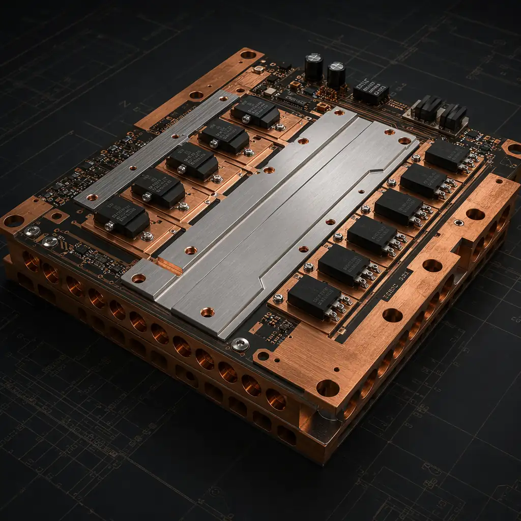
IGBT/MOSFET power stage boards for arc and spot welders. Massive copper pours for 200A+ switching. Thick aluminum substrate option for direct heatsink mounting.
Laminated copper bus bars embedded within PCB for power distribution at 200A+. Replaces discrete bus bars with integrated solution. Custom cross-section on request.
High-density control logic on 1oz signal layers with 6oz power layers in the same board. Server VRM, motor controller, and DC-DC converter applications.
Manufacturing Process
Heavy copper processing requires specialized etch techniques. Standard alkaline etch that works for 1oz copper would undercut 12oz traces by 6-8 mil per side. We use optimized etch compensation, the phototool has wider traces to account for lateral etching, and step-plating where copper is built up in multiple plating cycles for uniform thickness control.
BMS, cell interconnect, on-board charger, DC-DC converter
Server VRM, telecom rectifier, UPS inverter
Arc welder, spot welder, plasma cutter power stage
Inverter, MPPT charge controller, grid-tie converter
VFD, servo drive, motor controller IGBT module
Traction inverter, auxiliary power, wayside power
Tell us your copper weight, layer count, and current requirements. We'll review your design for heavy copper manufacturability and provide a detailed quote within 24 hours.

Tell us copper weight, layers, current, and quantity. Free DFM within 24h.