
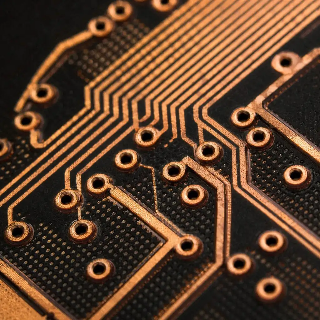
PCB Types / HDI PCB
High-Density Interconnect PCBs built with laser-drilled microvias as fine as 75µm, enabling 0.3mm BGA pitch and 3/3mil trace routing. From 1+N+1 to any-layer ELIC: every HDI configuration, certified to IPC Class 3.
Technology Overview
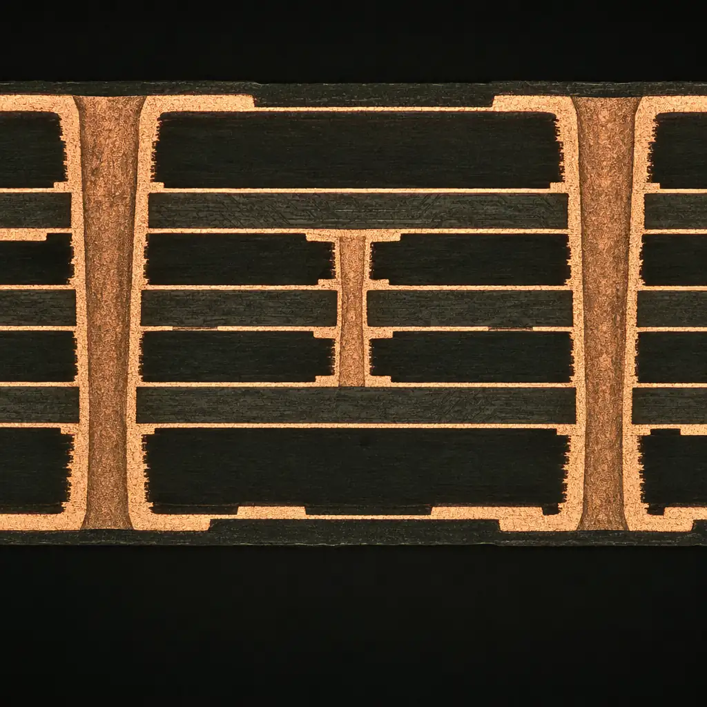
HDI (High-Density Interconnect) PCBs, defined by IPC-2226, use laser-drilled blind and buried microvias to achieve connection densities impossible with conventional through-hole technology. By replacing large plated through-holes with microvias as small as 75µm, HDI frees up routing space, reduces layer count, and enables compact designs with fine-pitch BGAs.
Our HDI capability spans the full range, from simple 1+N+1 build-ups for consumer wearables to complex any-layer ELIC (Every Layer Interconnect) structures for 5G base stations and aerospace modules.
Technical Specifications
| Number of Layers | 4 – 24 layers (evaluation required above 24L) |
| HDI Build-up Types | 1+N+1 · 2+N+2 · 3+N+3 · Any-Layer ELIC (up to 6-order) |
| Laser Via (CO₂) | 75µm (3 mil) standard; 50µm UV for thin dielectrics |
| Min. Trace / Space | 3 / 3 mil (0.075 / 0.075 mm); 2/2 mil with 1/3 OZ base copper |
| Min. BGA Pitch | 0.3 mm (via-in-pad with copper fill & planarization) |
| Min. Mechanical Drill | 0.15 mm (CNC) |
| Via Fill | Copper-filled (conductive) or resin-filled & capped (non-conductive via-in-pad) |
| Min. Annular Ring | 3 mil (laser via); 4 mil (mechanical via) |
| Aspect Ratio | Up to 14:1 (through-hole); evaluate if greater |
| Board Thickness | 0.1 – 4.0 mm (evaluate <0.2 mm or >3.5 mm) |
| Max. Panel Size | 500 × 600 mm (standard); up to 609 × 889 mm evaluation |
| Copper Weight (finished) | 18 – 70 µm (0.5 – 2 OZ); inner up to 3 OZ |
| Solder Mask | Green, Black, White, Red, Blue, Yellow; min. bridge 3 mil |
| Surface Finishes | ENIG · ENEPIG · Immersion Ag · Immersion Sn · OSP · HASL (Pb-free) |
| Base Materials | FR-4 · High-Tg FR-4 (170°C / 180°C) · Halogen-Free · BT · ABF |
| Impedance Control | ±5% (single-ended); ±5% (differential); TDR report included |
| Quality Standard | IPC-A-600 Class 2 / Class 3 · IATF 16949 · ISO 9001 |
Single build-up layer on each side. One set of blind vias connecting L1-L2 and L(N)-L(N-1), plus buried/thru-hole vias in the core. Cost-optimized for consumer and IoT applications requiring 0.5-0.8mm BGA pitch.
Two build-up layers per side with stacked or staggered microvias. Supports 0.4-0.5mm BGA pitch. Common in smartphones, automotive ADAS, and high-density industrial controllers.
Three sequential build-ups on each side. Enables 0.35mm BGA pitch with via-in-pad copper fill. Used in advanced mobile processors, FPGA carriers, and medical imaging modules.
Every layer interconnect. Any copper layer can connect directly to any other. Maximum routing density for 0.3mm BGA pitch designs. Our 24-layer 6-order ELIC process has been successfully qualified for aerospace and 5G base station applications.
Manufacturing Process
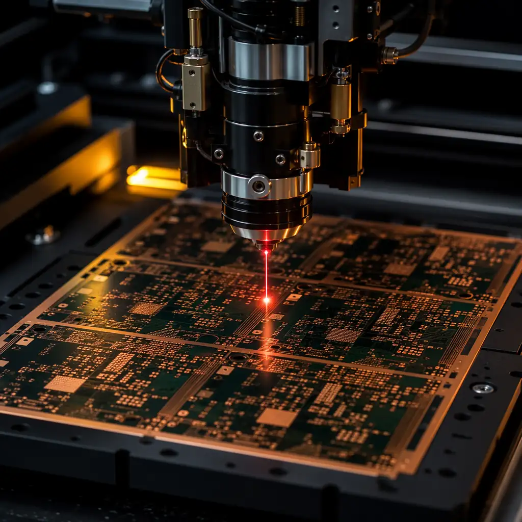
HDI manufacturing begins where conventional PCB fabrication ends, with the laser drill. Our CO₂ lasers create 75µm blind vias through thin dielectric layers with ±10µm positional accuracy. For ultra-thin dielectrics below 35µm, UV lasers achieve 50µm via diameters.
Any-layer ELIC main boards, 0.3mm BGA pitch, ultra-thin 0.6mm total thickness
Radar/lidar sensor PCBs, camera modules, 2+N+2 with high-Tg FR-4, IATF 16949
Ultra-compact 1+N+1, 0.4mm finished thickness, flex-rigid HDI hybrids
Hearing aids, implantable sensors, diagnostic imaging, IPC Class 3 mandatory
Satellite communication modules, 24L any-layer, Class 3 with QPL materials
Baseband units, massive MIMO antenna carriers, hybrid HDI + high-frequency
Send your Gerber files and stack-up requirements. Our engineering team will review your design for HDI manufacturability and respond with a detailed quote within 24 hours: including a free DFM report.

Tell us your layer count, HDI build-up type, BGA pitch, and quantity. Free DFM review within 24 hours.