
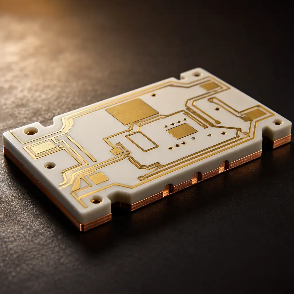
PCB Types / Ceramic PCB
When FR-4 melts at 130°C and aluminum MCPCB can't handle 400°C operating temperatures, ceramic PCBs take over. Alumina (Al₂O₃) and aluminum nitride (AlN) substrates with thick-film or direct-bonded copper metallization, for UV LEDs, IGBT power modules, and hermetic packaging.
Technology Overview
Ceramic PCBs use aluminum oxide (Al₂O₃, alumina) or aluminum nitride (AlN) as the insulating substrate instead of FR-4 or polyimide. These ceramics offer thermal conductivity 20-100× better than FR-4, can operate at temperatures exceeding 400°C, and provide a hermetic (moisture-impermeable) platform for sensitive electronics.
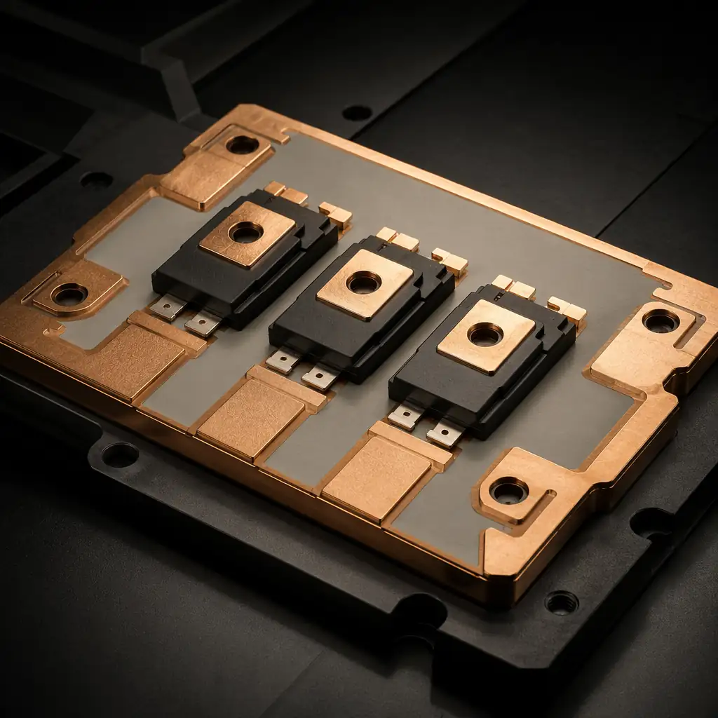
Three metallization technologies serve different needs: DBC (Direct Bonded Copper) for thick copper power applications, DPC (Direct Plated Copper) for fine-line resolution, and AMB (Active Metal Brazing) for AlN substrates where DBC doesn't bond well.
Technical Specifications
| Substrate Materials | Al₂O₃ 96% (20-24 W/m·K) · AlN (170-230 W/m·K) · ZTA · BeO (evaluation) |
| Metallization Types | DBC (Direct Bonded Copper) · DPC (Direct Plated Copper) · AMB (Active Metal Brazing) · Thick-Film Au/Ag/PdAg |
| DBC Copper Thickness | 100 – 300 µm (0.1 – 0.3 mm); 200/300µm most common |
| DPC Copper Thickness | 10 – 100 µm with additional plating build-up; Ti adhesion + Ni/Au finish |
| Min. Trace / Space (DPC) | 1 / 1 mil (25 / 25 µm), semiconductor-grade resolution |
| Min. Trace / Space (DBC) | 8 / 8 mil (0.2 / 0.2 mm), limited by thick Cu etch |
| Substrate Thickness | 0.25 – 1.0 mm (Al₂O₃); 0.38 – 1.0 mm (AlN); 0.38/0.63mm standard |
| Surface Finish | ENIG (<2µ") · ENEPIG · Immersion Ag · Ni/Au (electrolytic) · Wire-bondable Au |
| Via / Through-Hole | Laser-drilled 0.2-0.5mm; filled with Ag/PdAg or Cu/Ni/Au |
| Max Panel Size | 120 × 120 mm (standard); up to 190 × 140 mm evaluation |
| Quality Standard | IPC-6012 Class 3 · MIL-PRF-38534 (hermetic) · IATF 16949 · ISO 9001 |
Copper foil is directly bonded to ceramic at 1065°C using a copper-oxygen eutectic. Thick copper (up to 300µm) handles high current. Standard for IGBT power modules, EV/HEV traction inverters, and industrial motor drives.
Thin-film sputtering of Ti/Cu seed layer followed by electrolytic Cu plating. Achieves 1/1 mil trace resolution, semiconductor-grade. Used in UV LED submounts, laser diode carriers, and high-density ceramic interposers.
Active metal (typically Ti or Zr) braze paste bonds copper to AlN ceramic at ~900°C. Necessary because DBC doesn't bond well to AlN. Enables AlN's superior thermal conductivity for SiC MOSFET and GaN HEMT power modules.
Conductor paste screen-printed onto ceramic and fired at 850°C. Lower cost than DPC for medium-resolution designs. Used in hybrid microcircuits, resistor networks, and sensor substrates.
Manufacturing Process
The DPC process begins with sputtering a thin titanium adhesion layer followed by a copper seed layer onto the ceramic substrate. Photolithography defines the circuit pattern with semiconductor-grade resolution. Electrolytic copper plating builds the traces to the target thickness (typically 30-70µm), followed by Ni/Au finish for wire bonding and soldering. The result: 1-mil traces on a substrate that can handle 400°C.
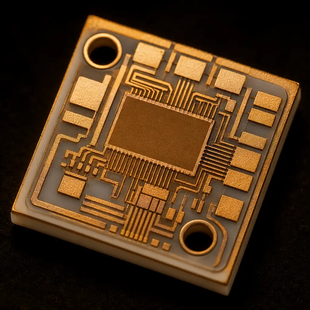
UV-C sterilization, horticulture COB, laser diode submount
IGBT, SiC MOSFET, GaN HEMT, IPM module base plate
Thick-film RF hybrid, T/R module, LNA substrate
Hermetic package, radar T/R, space-grade DC-DC converter
EV inverter IGBT substrate, OBC power module, 48V DCDC
Pressure sensor, gas sensor, flow sensor, biosensor substrate
Tell us your substrate material, metallization type, and thermal requirements. Our ceramic PCB specialists will review your design and provide a detailed quote within 24 hours.

Tell us substrate, metallization, thermal requirements, and quantity. Free review within 24h.