

Capabilities / PCB Fabrication / Standard PCB
From single-sided prototypes to 32-layer production boards. Industry-standard FR-4 with High-Tg, halogen-free, and high-CTI variants. Every board 100% AOI inspected, E-tested, and built to IPC-A-600 Class 2/3.
FR-4 remains the workhorse of the PCB industry, but not all FR-4 is the same. We stock multiple grades to match your application requirements, from cost-optimized consumer-grade laminates to high-reliability materials for automotive and industrial environments.

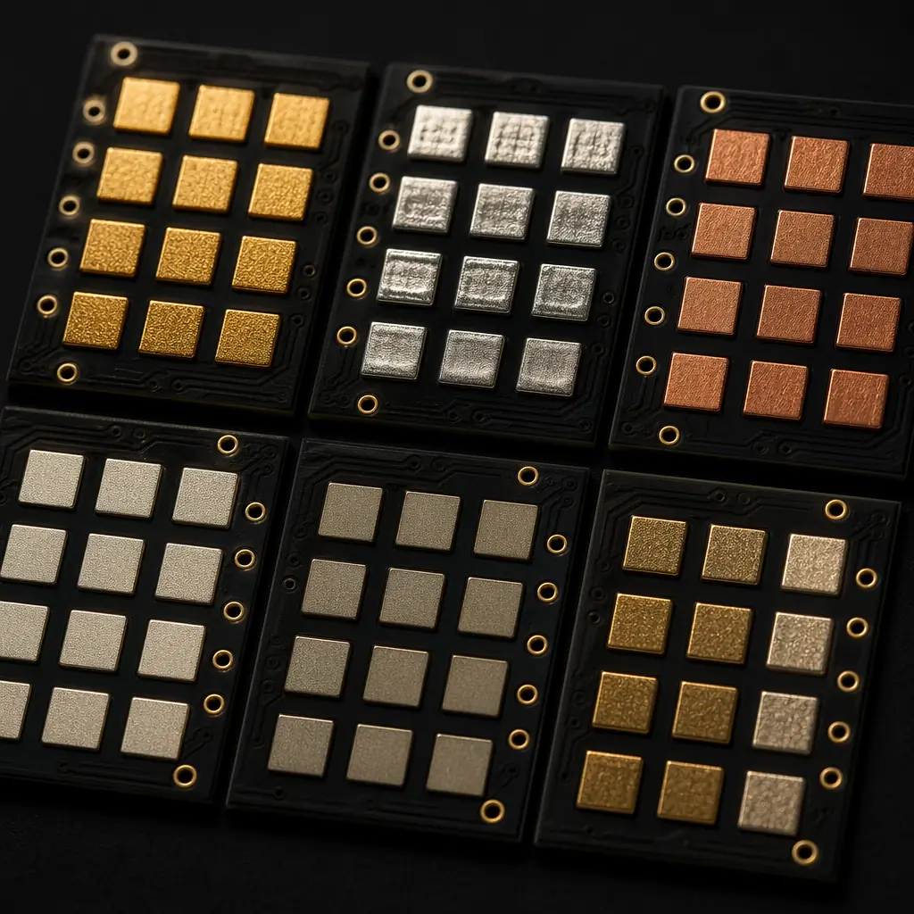
| Finish | Thickness | Planarity | Shelf Life | Best Application |
|---|---|---|---|---|
| ENIG | Ni 3-6µm, Au 0.05-0.15µm | Excellent | 12 months | Fine-pitch BGA, general purpose, most popular |
| HASL (Lead-Free) | 1-40µm | Uneven | 12 months | Through-hole, cost-sensitive, wide compatibility |
| OSP | 0.2-0.5µm organic | Excellent | 6 months | Cost-sensitive SMT, short shelf-life acceptable |
| Immersion Silver | 0.15-0.5µm | Excellent | 6-12 months | High-frequency RF, low signal loss |
| Immersion Tin | 0.8-1.2µm | Excellent | 6 months | Press-fit connectors, fine-pitch flat pads |
| Hard Gold | Ni 3-6µm, Au 0.5-1.5µm | Excellent | 24 months | Edge connectors, keypads, high-cycle durability |
| ENEPIG | Ni+Pd+Au stack | Excellent | 12 months | Wire bonding, press-fit, high-reliability |
Beyond the standard green mask, we offer 10+ solder mask colors and 3 silkscreen color options. LPI (Liquid Photo-Imageable) solder mask with 0.1mm minimum dam width as standard, 0.075mm available for advanced designs. Matte finish options provide excellent contrast for AOI inspection.
| Category | Available Colors | Gloss/Matte |
|---|---|---|
| Solder Mask | Green, Blue, Black, White, Red, Yellow, Purple, Matte Green, Matte Black, Transparent | Both available |
| Silkscreen/Legend | White, Black, Yellow | , |
| Peelable Mask | Blue, White (temporary wave-solder masking) | , |
| Method | Description | Best For |
|---|---|---|
| V-Scoring | V-groove cuts on both sides, leaving a thin web for snap-out depanelization. 30/45/60 angles. Remaining thickness 0.3-0.5mm. | Rectangular boards, high-volume, cost-effective |
| Tab Routing | Routed outline with breakaway tabs (mouse bites). 5-8 perforated tabs per board side. No stress on components. | Irregular shapes, heavy components, medium volume |
| Full Routing | Complete CNC rout with zero-connection separation. Boards delivered fully singulated. | Complex outlines, high-value boards, clean edges required |
| Mixed V-Score + Route | Combined approach, V-score on straight edges, route on curves. Optimizes cost and quality. | Boards with mixed straight and curved edges |
Standard panel utilization: 80-90%. Custom panel arrays with fiducials, tooling holes, and coupon positions included by default. See our DFM panelization guide.
| Volume Tier | Quantity | Typical Lead Time | Pricing Model |
|---|---|---|---|
| Prototype | 5-50 pcs | 5-7 days (standard), 24-72h (rush) | Per-order NRE + unit cost |
| Small Batch | 50-500 pcs | 7-10 days | Unit cost, declining with volume |
| Medium Volume | 500-5,000 pcs | 10-15 days | Panel-optimized, fixture tooling NRE applies |
| Mass Production | 5,000-100,000+ pcs | 15-25 days | Per-panel pricing, annual contract available |
Upload your design files, include layer stackup, material preference, surface finish, and quantity. Our engineering team responds within 24 hours with a detailed DFM analysis and quote. No commitment required.
Upload Gerber + BOM, 24h quote with free DFM review.