
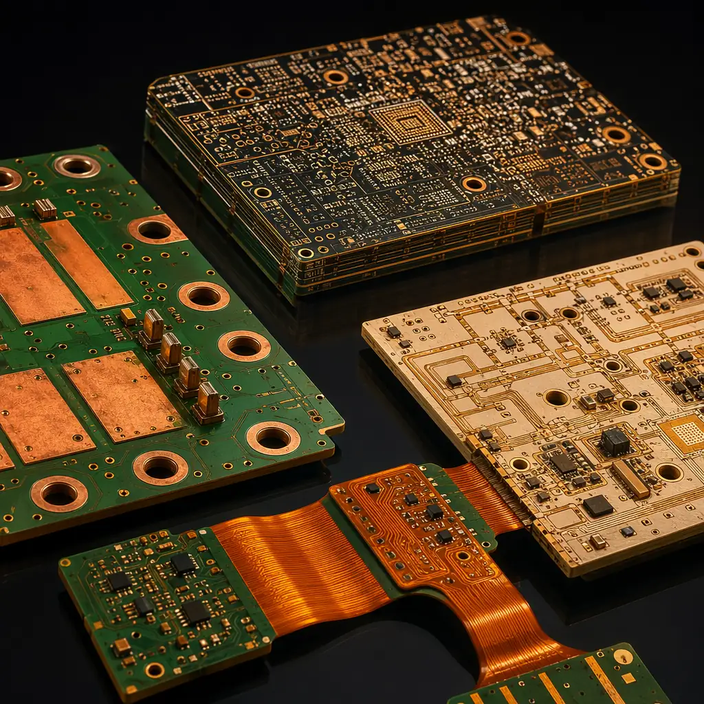
Capabilities / Advanced PCB
HDI any-layer, flexible circuits, rigid-flex hybrids, Rogers/PTFE high-frequency laminates, heavy copper up to 12oz, ceramic substrates, and advanced processes like back-drilling and via-in-pad. Every board manufactured in-house to IPC Class 3 standards with full traceability.
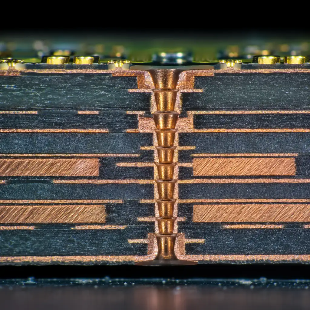
HDI Technology
HDI PCBs use laser-drilled microvias (as small as 75µm) to connect layers with far greater density than traditional through-hole vias. Our any-layer HDI process, also known as "every-layer interconnect" or ELIC, allows any layer to connect to any other layer directly, maximizing routing freedom in compact designs.
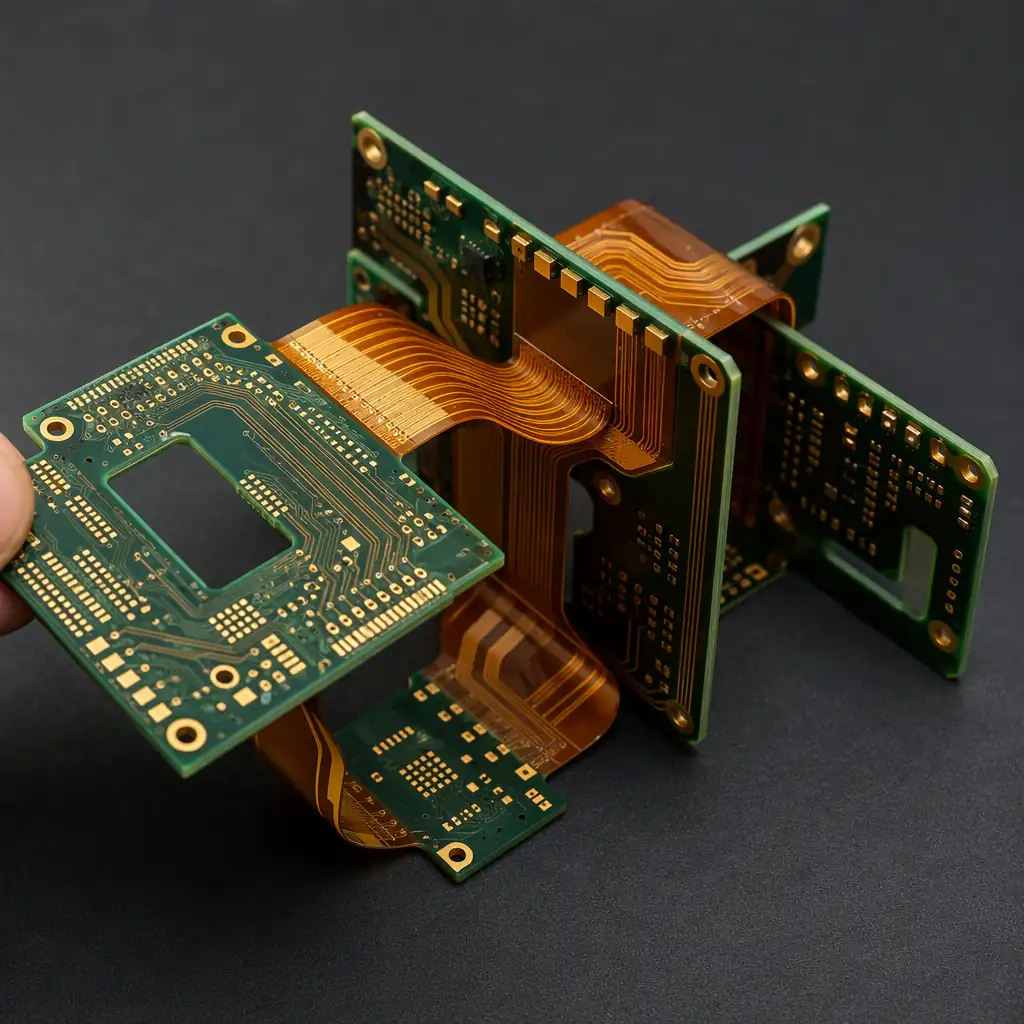
Flexible & Rigid-Flex
Flexible PCBs replace bulky wiring harnesses and connectors. Rigid-flex combines rigid board sections with flexible interconnects in a single, foldable assembly, eliminating connectors, reducing weight, and improving reliability in space-constrained applications.
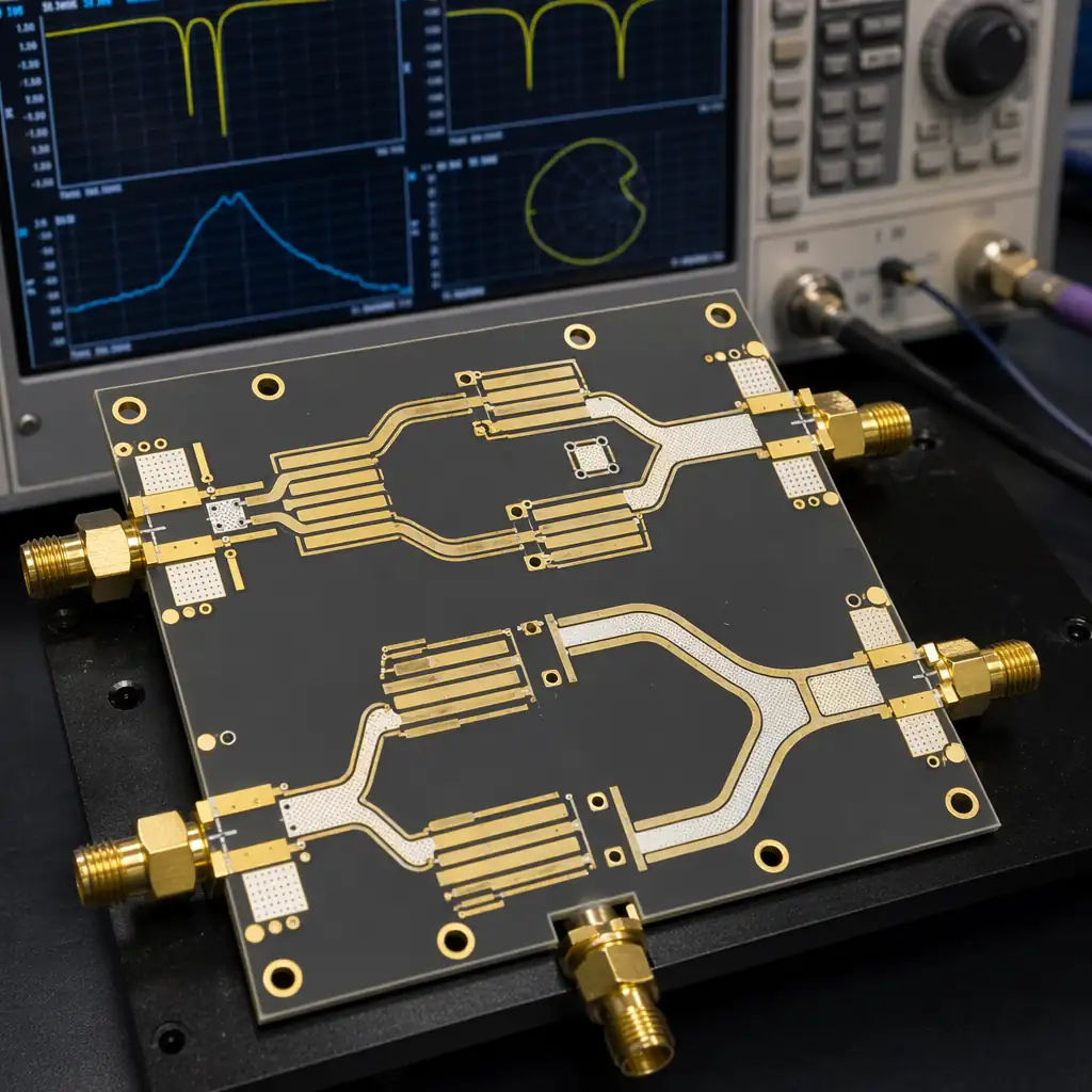
High-Frequency / RF
When every dB of loss matters, the laminate defines performance. We stock Rogers, Taconic, Arlon, and Isola low-loss materials, and we precision-machine RF structures with ±5% impedance control verified by TDR on every controlled-impedance panel.
| Technology | Standard | Medium | Advanced | On Request |
|---|---|---|---|---|
| Layer Count | 1–14 | |||
| Layer Count (Advanced) | , | 16–24 | ||
| HDI Type | 1+N+1 | |||
| Any-Layer HDI | , | 4–12L | ||
| Flex PCB | 1–2L | |||
| Rigid-Flex PCB | , | 4–10L | ||
| FR-4 (Standard Tg) | , | , | ||
| High-Tg FR-4 / Halogen-Free | , | |||
| Rogers 4000 Series | , | , | ||
| PTFE (Taconic/Arlon) | , | , | ||
| Ceramic (Al₂O₃/AlN) | , | , | ||
| Aluminum MCPCB | , | , | ||
| Copper Weight 0.5–3oz | , | |||
| Copper Weight 4–8oz | , | , | ||
| Copper Weight 10–12oz | , | , | ||
| Trace/Space 5/5mil+ | , | |||
| Trace/Space 3/3mil | , | , | ||
| Aspect Ratio ≤8:1 | , | |||
| Aspect Ratio 10–16:1 | , | , | ||
| Back-Drill | , | , | ||
| Via-in-Pad (VIP) | , | , | ||
| Edge Plating | , | , | ||
| Gold Fingers 30–50µ" | , | |||
| ENIG / ENEPIG | , | |||
| Impedance ±10% | , | |||
| Impedance ±5% | , | , |
Heavy Copper
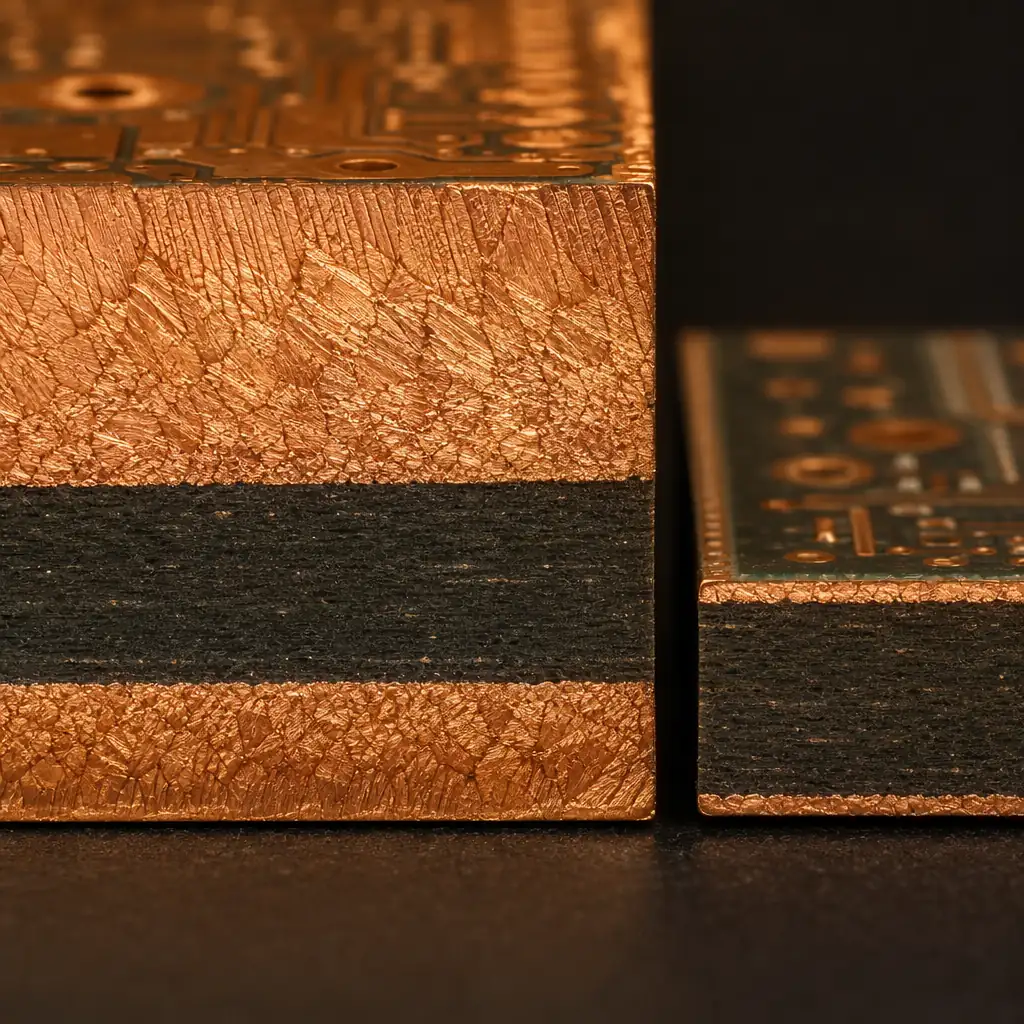
Heavy copper PCBs carry tens to hundreds of amperes while keeping temperature rise within safe limits. Our extended plating process builds copper thickness evenly across the board, inner and outer layers, with controlled profile uniformity verified by cross-section microscopy on every lot.
Send your stackup, layer count, material preferences, and any special process requirements. Our senior engineers will review feasibility and return a detailed manufacturing plan within 24 hours.

Upload your Gerber files and requirements. Free review within 24 hours.