

A solder mask dam is the narrow strip of cured mask that sits between two adjacent copper features and stops molten solder from joining them. It is the cheapest feature on the board to design correctly and one of the most expensive to get wrong, because a dam that is too thin does not fail at fabrication, it fails at reflow, and by then the panels are already made. A sliver is what remains when the web is thinner than the process can hold: a free-standing flake of mask that will lift, land on a neighbouring pad, and be read as a bridge by the first AOI pass.
The question designers and DFM reviewers actually bring to a fabricator is not what a dam is. It is how thin the web can go at a given pad pitch before the design stops being manufacturable, and who carries the cost when it does not. This page sets out the minimum width for each mask thickness, the pitch at which the dam physically cannot exist, and an accept-or-reject framework for the slivers that do get made.
What a Dam Actually Is
The mask is not printed on copper. It is printed on laminate between copper features, or on top of a copper plane where there is no pad. That distinction matters because the adhesion of cured LPI to bare laminate is weaker than its adhesion to copper, and the sidewall of a dam during development is a vertical face that the developer is trying to wash past without undercutting it. A dam is therefore a narrow, free-standing wall of polymer standing on the weakest surface available, and its width is bounded by how tall that wall is relative to its base.
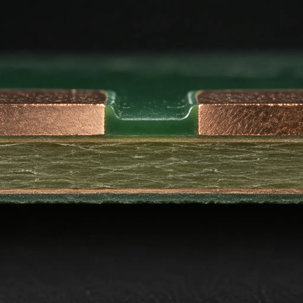
The web between these pads is mask on bare laminate, not mask on copper. Its sidewalls are vertical, and the developer must clear them without undercutting the base.
There are three dam geometries on a typical board, and they are not equally demanding. Pad-to-pad is a dam between two features at the same height, usually the fine-pitch case. Pad-to-trace is a dam between a pad and a routing trace, where the copper on one side is thin and the mask has less to anchor to. Trace-to-trace is a dam between two parallel traces under mask, and in that case the mask is simply a conformal cover and the width hardly matters, because nothing is being separated at reflow.
Only the first two are real constraints. When a designer asks for a 0.05 mm dam over a trace routing channel, they are usually asking for something that carries no process risk and costs nothing. When they ask for the same 0.05 mm between two 0.4 mm pitch pads, they are asking for a sliver.
Minimum Dam Width by Mask Thickness
The minimum width is not a single number. It scales with the cured thickness of the mask, because a taller wall needs a wider base to stay attached through development, cure and the thermal shock of reflow. The table below is the process floor we work to on LPI, and it is the number that should appear on a fabrication drawing rather than a general "minimum dam 0.1 mm" note copied from a template.
| Cured mask thickness | Minimum dam, pad-to-pad | Minimum dam, pad-to-trace | Practical note |
|---|---|---|---|
| 15 to 25 microns (thin LPI) | 0.075 mm | 0.075 mm | Feasible on fine pitch, higher sliver risk at the low end of the range |
| 25 to 40 microns (standard LPI) | 0.100 mm | 0.100 mm | The default callout for most boards |
| 40 to 60 microns | 0.125 mm | 0.100 mm | Thick mask for high voltage or harsh environment |
| 60 microns and above | 0.150 mm | 0.125 mm | Matt or high-build mask, sidewalls dominate |
Two rows in that table carry more weight than the others. The 0.075 mm row is where a fabricator will accept the design but tell you the yield is variable, and a variable yield on a fine-pitch board is a cost that appears in the price eventually. The 0.100 mm row is the callout that most designs should carry, because it holds across thickness variation and does not depend on the operator running the coater at the thin end of the window.
Thickness itself is not constant across the board. Mask pools at the edge of a large copper pour and thins over a dense array of fine traces, because the screen or the spray deposits by area, not by feature. A design that nominally carries 30 microns of mask may have 20 microns between the pads in the densest region and 45 microns at the board edge. The dam width has to work at the thin end of that distribution too, because a thinner wall between two pads is also a wall that develops faster and undercuts sooner.
The Pitch Ceiling
Below a certain pitch, the dam stops being small and starts being absent. The arithmetic is simple: pitch minus pad width minus two times the mask registration tolerance equals the available web. At 0.5 mm pitch with 0.25 mm pads and 0.05 mm registration allowance, the available web is zero, and the design has to decide whether the mask defines the pad at all.
| Pitch | Typical pad width | Registration allowance | Available web | What the mask should do |
|---|---|---|---|---|
| 0.65 mm and above | 0.35 mm | 0.05 mm | 0.15 mm | Normal dam, standard callout |
| 0.50 mm | 0.25 mm to 0.30 mm | 0.05 mm | 0.10 mm to 0.15 mm | Dam at 0.10 mm, thin LPI |
| 0.40 mm | 0.20 mm | 0.05 mm | 0.10 mm | Dam at 0.075 mm to 0.10 mm, tight window |
| 0.30 mm and below | 0.15 mm | 0.05 mm | Zero to 0.05 mm | No dam possible. Tented or open vias, NSMD pads, mask defined by aperture |
The last row is the one that produces most of the arguments. When the available web is zero, no amount of claiming a 0.05 mm dam will make one exist, and a design that insists on it will be built either with a mask-defined pad that is smaller than the copper, or with a sliver that the fabricator removes by hand. Neither is what the designer intended, and only one of them is documented.
The practical move at 0.3 mm pitch and below is to stop treating the mask as a feature between pads and treat it as a coating over everything that is not a pad. That means defining pads by the mask aperture, accepting that the copper is larger than the opening, and confirming that the assembly house can live with mask-defined pads on that footprint. SMD versus NSMD pad definition is a whole separate decision with its own reliability consequences, covered in our page on SMD vs NSMD pad definition, and it should be made together with the dam callout rather than after it.
Sliver: When the Web Is Too Thin to Be a Dam

A sliver is a dam that survived fabrication and will not survive reflow. Its failure mode is mechanical, not electrical: it lifts, travels, and lands.
A sliver is a narrow strip of mask that is attached at one or both ends but unsupported along its length. It can come from a design that specified a web below the process floor, from a registration error that left a mask edge hanging over an opening, or from a defect in the artwork where two apertures nearly touch. All three produce the same physical result: a thin polymer beam with almost no adhesion area, spanning a gap that will see thermal expansion of the copper underneath it.
What makes a sliver worse than a missing dam is that it is a contamination source. At reflow the mask softens, the copper expands more than the mask, and the beam lifts. From there it has three destinations, and all of them are bad. It can stand up and shadow a pad from the paste deposit. It can fall across two pads and be read as a bridge at AOI, which will then be reworked, adding a handling cycle to a board that had nothing wrong with its solder. Or it can flake off entirely and travel inside the assembly, which on a board that later gets conformal coated becomes a coating defect under a component.
A fabricator has only two honest options when the artwork produces slivers: strip and remake the artwork, or build it with a concession and accept a lower yield. Hand removal is not an option on fine pitch, because the act of removing a sliver damages the adjacent mask edge and creates a second defect of the kind that mask type and chemistry choice was meant to prevent.
Accept or Reject: The Verdict Framework
The acceptance question is not "is there a sliver" but "is the sliver isolated from a conductor surface that it can bridge to, and is it attached". That framing comes from the way visual acceptance standards treat mask features: a cosmetic irregularity in a non-conductive area is one thing, and a mask fragment that stands between two pads with a solder deposit arriving is another.
| Condition | Class 1 | Class 2 | Class 3 | Action |
|---|---|---|---|---|
| Isolated mask irregularity, not between conductors | Accept | Accept | Accept | None |
| Sliver attached at both ends, outside a solderable area | Accept | Accept with note | Reject | Document, monitor yield |
| Sliver attached at one end, adjacent to a pad | Accept with note | Reject | Reject | Rework only if accessible, otherwise scrap |
| Sliver bridging or partially bridging two pads | Reject | Reject | Reject | Scrap or remake artwork |
| Dam absent where the drawing specified one | Reject if functional | Reject | Reject | Fix the artwork, not the panel |
The class columns are the part buyers miss. A design built to Class 2 acceptance cannot absorb a one-end-attached sliver next to a pad, even though the same board built to Class 1 could ship with a note. On a high-reliability programme the class is fixed by the customer, so the design must clear the Class 3 row before the first panel exists, and there is no concession path afterwards.
Two pieces of evidence should be requested with every lot where a mask feature was flagged. First, the artwork revision that produced the panel, so the sliver can be traced to a specific aperture definition rather than to "the coater". Second, a photograph with a scale reference, because a sliver measured at 0.04 mm and one measured at 0.09 mm sit on opposite sides of the verdict table on some designs. Without the scale, the argument becomes one person's impression against another's.
Specifying It in the Fabrication Drawing
A single line in the fabrication notes removes most of this risk. The note needs three elements: the minimum dam width, the mask thickness it applies at, and the instruction for what to do when the web falls below the minimum. The third element is the one that is usually missing, and it is the one that decides whether a fabricator silently builds a sliver or calls you.
Useful wording is short and testable: minimum solder mask dam 0.10 mm at a cured thickness of 25 to 40 microns; where the pad pitch does not permit a 0.10 mm dam, mask-defined pads are permitted and the aperture becomes the pad definition; report any sliver adjacent to a solderable area before fabrication proceeds. That last clause converts a downstream scrap into an upstream review, which is the entire point of a DFM note.
The mask thickness callout itself is worth pinning down rather than leaving to the solder mask type default, because the dam minimum moves with it and because thickness is also the input to the registration tolerance in the pitch table above. A drawing that specifies dam width without thickness is specifying half a constraint, and it will produce a conversation at the first build rather than an answer.
Our DFM review runs the dam check against pad pitch and mask thickness before tooling, and reports the apertures that cannot hold the specified web rather than building them and sorting afterwards. For the wider set of checks that run alongside it, the shift-left DFM verification page describes the review sequence. If you have a fine-pitch footprint where the mask callout is still open, send the pad definitions through the quote form and we will return the dam width the artwork can actually hold.