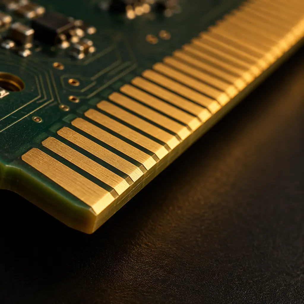
Almost every card-edge failure I have reviewed in the last four years started at the same place: the very bottom edge of the board, on the two faces that meet the connector's first contact spring. Not in the middle of the gold, not at the tip of a long trace. At the bevel. Engineering teams spend their review time on gold thickness and plating hardness, and then accept whatever bevel the fabricator's routing program happens to produce.
That is the wrong order of attention, and the reason is mechanical rather than chemical. Gold thickness governs how long a contact surface survives abrasion. Bevel geometry governs whether the surface gets damaged at all during insertion, and whether the contact spring is compressed gradually or struck. A board with 30 micro-inches of hard gold and a badly formed 20 degree bevel will show contact resistance drift well before a board with 15 micro-inches and a proper chamfer.
This article works through the mechanics of the insertion edge, then converts it into the small number of lines that belong on a fabrication drawing. If you are still choosing between finishes, the hard gold vs soft gold vs ENIG comparison covers the material decision; this page assumes hard gold and covers the geometry that makes it work.
Why the Bevel Decides Connector Life
A card-edge connector is a spring loaded against a plated surface. When the board enters, each contact spring rides up the bevel and is deflected outward by an amount called the interference. It then travels along the finger on a short rubbing stroke called the wipe, and finally parks on its contact area. Three things can go wrong in that sequence, and all three are functions of the edge.
Stubbing on the leading face
If the chamfer is too shallow or has a burr, the leading face presents a nearly square corner to the contact spring. The spring does not ride up, it collides. This is the classic stubbed contact, and on a multi-row connector a single stubbed spring can be bent permanently out of its working range in one insertion. Once bent, that row never makes reliable contact again, and the failure appears later as an intermittent channel that survives every bench test.
Under-deflection from insufficient bevel depth
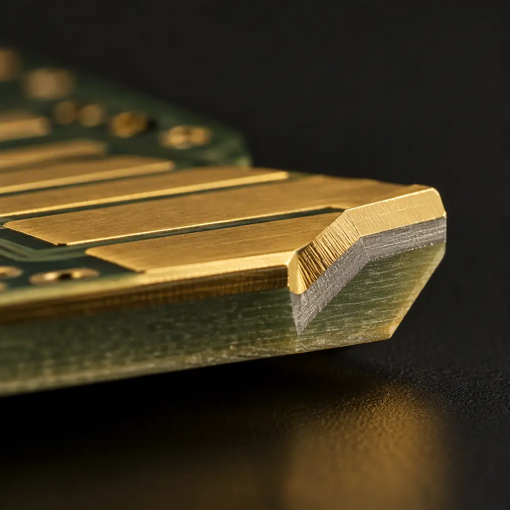
Bevel depth, measured along the board surface from the edge to where the full board thickness begins, sets how gradually the spring is loaded. The rule of thumb our process engineers work to is a bevel depth of at least 0.3 mm per 1.6 mm of board thickness, so a 1.6 mm card gets 0.30 to 0.50 mm of chamfer on each face. At 2.0 mm thickness the chamfer should reach 0.40 to 0.60 mm. Under-cutting below that ratio concentrates the entire deflection into a very short ramp and multiplies the peak local stress on the gold.
Burrs and smeared plating at the chamfer
The bevel is cut after plating on most volume processes, either by a router with a V-bit or by a dedicated chamfering machine. Routing cuts through 3 to 5 micrometres of nickel and 0.4 to 1.3 micrometres of gold, and it drags material. A dull bit leaves a burr of nickel and gold on the chamfer face that is both a short-circuit risk between adjacent fingers and an abrasive particle for the connector. This is why bevel quality must be an inspection item, not just a drawing note.
Bevel Angles: What Each One Costs You
The industry default is a 30 degree chamfer measured from the board plane, and it exists because it is fast to cut and forgiving of thickness variation. It is also the angle that produces the highest insertion force per unit of contact deflection. Steeper angles, meaning 20 or 15 degrees from the board surface, load the spring more gradually and are the right choice wherever the connector is inserted by hand or by a service technician rather than by a controlled press.
Gold Thickness by Mating Cycle Class
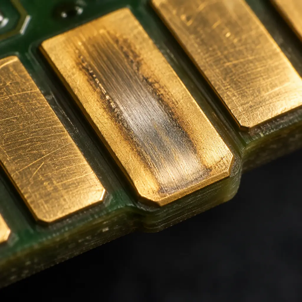
Gold does not wear away in a uniform film. Under a loaded sliding contact it wears at the edges of the contact track first, exposing the nickel barrier, and nickel oxide then drives contact resistance up by an order of magnitude. The practical life of a finger is therefore set by gold thickness, contact force and wipe length acting together, which is why thickness alone does not predict cycle life and why suppliers quoting only thickness are quoting an incomplete answer. The hard vs soft gold guide explains the hardness side, Type II at 130 to 200 Knoop on a standard nickel barrier; this table gives the thickness-to-cycles relationship that our customers use for specification.
| Mating cycles required | Gold thickness (hard gold) | Typical application | Notes |
|---|---|---|---|
| Under 50 | 0.25 to 0.5 micrometre (10 to 20 micro-inches) | Fixed internal riser cards, one-time assembly | Service access must be defined as non-mating |
| 50 to 500 | 0.75 micrometre (30 micro-inches) | Consumer edge connectors, add-in modules | Specify wipe of at least 1.0 mm |
| 500 to 5,000 | 1.0 to 1.3 micrometre (40 to 50 micro-inches) | Rack-mount equipment, backplane blades | Mandatory bevel inspection, tape pull per lot |
| Over 5,000 | 1.3 to 2.5 micrometre (50 to 100 micro-inches) | Test fixtures, burn-in sockets, mating connectors | Nickel barrier 3 to 5 micrometres, low-stress nickel |
Two numbers in that table are worth arguing about. First, the nickel barrier. Under 1.27 micrometres of nickel the barrier becomes porous at the grain boundaries and diffusion of copper to the surface accelerates, which is the mechanism behind the gold discoloration that buyers report as a plating defect. Specify 3 to 5 micrometres of nickel, and specify low-stress sulphamate nickel if the finger will be bent or the board will see thermal cycling. Second, gold purity. Hard gold is alloyed with cobalt or nickel at roughly 0.05 to 0.2 percent to raise hardness, and that alloy raises resistivity. For high-cycle test fixtures where contact resistance stability matters more than wear, a purer soft gold at greater thickness sometimes wins; the trade-off is in the finish selection page rather than here.
Contact Wipe: The Requirement Nobody Puts on the Drawing
Wipe is the distance the contact spring travels across the finger while loaded. It exists to push contamination and oxide out of the contact zone. If the finger is exactly as long as the contact's park position, wipe approaches zero and the connector relies entirely on the cleanliness of the gold at the moment of mating, which is a poor bet on a factory floor.
Practically, fingers should be designed so that the contact parks 1.0 to 1.5 mm past the wipe zone, and the finger should extend a further 0.5 mm beyond the park position so that minor board-to-connector registration error does not put the contact on the bevel ramp. On a 2.54 mm pitch edge connector, a finger length of 5.0 mm with 2.0 mm of bevel and 2.5 mm of usable contact area is a sound starting point. Our pad-to-hole and annular ring rules cover the same registration logic for drilled features if you want the general tolerance framework.
What a Card-Edge Fabrication Drawing Must State
The most common cause of a card-edge board arriving wrong is an incomplete drawing. Fabricators do not invent bevel angles; they run the standard one. Nine lines on a drawing prevent nearly every dispute we see:
Bevel geometry as a dimensioned callout
State the angle from the board plane and the depth on each face, for both top and bottom when fingers exist on both sides. Do not write "bevel gold fingers", which is not a specification.
Gold thickness and measurement method
Thickness with a tolerance and a method, for example 1.0 micrometre minimum hard gold measured by X-ray fluorescence at three points per finger group. Without a stated method, thickness is unverifiable in a dispute.
Nickel barrier thickness
3 to 5 micrometres, sulphamate low-stress type where the board will see thermal cycling. This single line prevents the mid-life discoloration complaints that get misdiagnosed as contamination.
Bevel surface quality
No burr, no smeared plating, edge chip under 0.2 mm, and the inspection method. Visual at 10x magnification on every panel is achievable and is the cheapest defect gate in the whole card-edge process.
Tape pull adhesion
Per lot, per finger group, with the tape grade and pass criterion. Gold that passes thickness but fails adhesion will lift at the bevel on the first insertion, and the failure will be attributed to handling.
The remaining four items are cheaper still: finger pitch and gap tolerance, solder mask clearance at the gold boundary, the plating resist method (dry film is preferred over screen printed resist for pitch under 1.0 mm), and a cross-section requirement through one finger showing nickel and gold layers. That cross-section is the only way to confirm the barrier thickness claim rather than the surface-only XRF reading. Our edge plating and castellation guide covers how sidewall plating interacts with the same process steps when the board needs both.
Inspection Gates That Actually Catch Bad Fingers
Three gates carry almost all of the value. The first is a 10x visual on the bevel before any electrical test, because a burr found there costs minutes to rework and a burr found at the customer costs a returned lot. The second is XRF thickness at the finger tips and mid-finger, because tip thickness runs 20 to 30 percent low on poorly controlled plating lines and the tip is where the first contact lands.
The third is contact resistance after a defined number of insertions, on a sample basis. This is the only test that measures the system rather than the coating, and for anything above 500 rated cycles it is worth the fixture cost. Boards that pass 50 insertions at under 20 milliohms and still pass at the rated cycle count are boards whose bevel, wipe and thickness are all in range together.
Handling deserves a sentence of its own. Gold fingers are the most abrasion sensitive feature on the board, and paper interleaving that slides across the bevel in a stack will scratch it. Ship card-edge boards with the fingers facing inward in the stack, in antistatic bags, and with a note on the box. The copper wrap and edge plating page covers the parallel concern for plated board edges that see mechanical wear.