
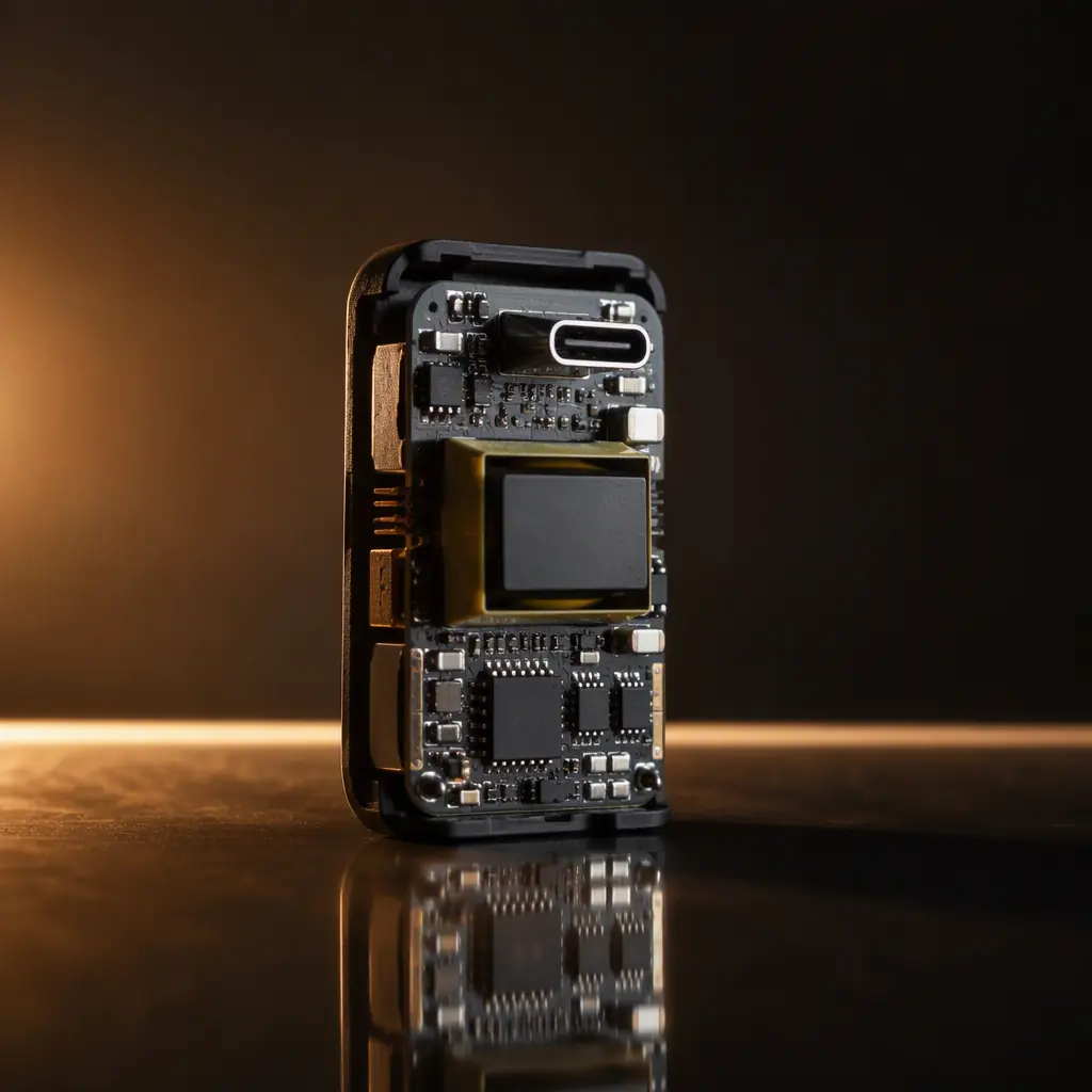
Gallium-nitride power devices have rewritten the USB charger market: a 65W GaN charger is smaller than the silicon charger that shipped with the same laptop five years ago, and USB PD 3.1 now pushes single-port supplies to 240W at 48V. GaN's low gate charge and near-zero reverse recovery let the converter switch at 300 kHz to 1 MHz instead of the 65-100 kHz of silicon flybacks, which shrinks the magnetic components dramatically — but it moves the engineering difficulty from the transformer into the PCB. At 1 MHz with <10 ns switching edges, layout parasitics that were invisible at 100 kHz become efficiency killers, EMI sources, and even reliability risks.
Huaxing PCBA manufactures GaN chargers and adapters for consumer, industrial, and automotive customers — 2-8 layer high-Tg stackups, 2 oz and heavier copper for the power path, controlled impedance on the USB signal pairs, and 8 SMT lines with X-ray inspection for the high-density primary side. This guide walks through topology selection, power-stage layout, thermal management, EMI control, USB PD routing, isolation rules, and the DFM specifications to put on the fabrication drawing.
Topology Choice: Flyback, Active Clamp, or PFC + LLC
The power architecture sets every downstream layout decision. The table below summarizes where each topology fits in 2026 GaN charger designs.
| Topology | Power Range | Switching Frequency | Typical Efficiency | Used In |
|---|---|---|---|---|
| Quasi-resonant flyback | 20-90W | 150-300 kHz | 90-93% | 65W phone/laptop chargers |
| Active-clamp flyback (ACF) | 65-140W | 300-700 kHz | 93-95% | Compact 100W+ single-port |
| Bridgeless PFC + LLC | 140-240W | PFC 100-300 kHz, LLC 300 kHz-1 MHz | 94-96% | 140-240W multi-port GaN |
QR Flyback for Cost-Driven 65W Designs
The quasi-resonant flyback with a GaN primary (typically 650V GaN in a 4×6 mm DFN) is the workhorse of the 65W segment. It uses valley switching to cut turn-on losses and needs no auxiliary switch, keeping BOM and layout simple. Design effort goes into the snubber and the transformer leakage inductance — a planar or well-coupled bobbin transformer with <1% leakage keeps the ringing under control. Our SMPS layout guide covers the general flyback layout rules this design builds on.
Active-Clamp Flyback for the 100W Class
Above 90W, the flyback's turn-off loss and leakage energy penalty grows, and the active-clamp flyback adds an auxiliary GaN or MOSFET to recycle the leakage energy. It recovers 1-2% efficiency and lets the converter run at 500-700 kHz with a smaller transformer — at the cost of a second switch, a clamp capacitor, and tighter layout discipline. The clamp loop (auxiliary switch + capacitor) must be a small, tight loop next to the transformer primary; inductance here directly increases voltage stress on the clamp switch.
PFC + LLC for 140W and Above
Above 140W, chargers need power-factor correction to meet EN 61000-3-2 harmonic limits, and the standard architecture is a boost PFC stage (often totem-pole bridgeless with GaN for 96%+ efficiency) followed by an LLC resonant converter. This is a two-board-class layout: the PFC section handles 240-400V DC with high dV/dt, and the LLC section runs at 300 kHz-1 MHz. Isolation, creepage, and thermal management become the dominant layout constraints. Our power integrity guide covers the PDN design these stages depend on.
Key Takeaway: Choose the topology by power level and enclosure size: QR flyback to 90W, active-clamp flyback to 140W, PFC + LLC above that. Each step up in frequency moves more design risk from the magnetics into the PCB layout.
Power Stage Layout: Loops, Gate Drive, and Copper
The power stage is where GaN boards live or die. The switching loop — high-side device, low-side device, and the decoupling capacitor across them — must be physically as small as possible.
Minimize the Power Loop Inductance
Every nanohenry in the half-bridge loop adds voltage overshoot at turn-off: V = L × dI/dt, and GaN switches dI/dt in the A/ns range. A loop inductance above 5 nH can push the switch-node voltage past the 650V rating on a 400V rail. Place the high-side and low-side devices and the bus capacitor so the loop is a single small square on one layer, with the return path directly underneath on the adjacent layer. Use multiple vias in parallel for every connection in the loop, and never route the loop through a long trace. Our trace width and current capacity guide gives the copper sizing math for the power path.
Keep the Gate Drive Path Short and Clean
GaN gate drivers are usually integrated in the same package as the power stage (half-bridge GaN ICs with driver, like the parts used in most modern chargers), which removes the external gate-loop problem. If you use discrete GaN devices, the driver must sit within 3-5 mm of the gate pad, the gate resistor directly at the device, and the drive return must not share the power-loop path. A separate Kelvin-source connection for the low-side device keeps the drive from being corrupted by the switching current. See our power integrity guide for decoupling placement rules.
Size the Copper for DC and Thermal, Not Just Resistance
A 140W charger at 28V/5A carries 5A on the secondary; at 48V/5A the primary average current is still 2-3A plus a large AC ripple component. Use 2 oz copper on the power layers as a baseline (Huaxing supports up to 6 oz), widen the traces for the ripple current, and duplicate critical paths across layers with via arrays. The switch node, in particular, needs enough copper to spread heat from the device into the board — a 12 mm² exposed-pad GaN IC wants a thermal pad pattern with a 3×3 or 4×4 via array directly under the pad, connected to an internal copper pour. Our thermal management guide details the via and pour design.
Key Takeaway: The power stage layout is a loop-minimization problem: tight switching loop, short gate drive, and copper sized for both current and heat. Measure the loop by its area — a small loop on one layer beats a spread-out loop on two.
Thermal Management: Dissipating 5-8W From a Matchbox
A 95% efficient 140W charger still dissipates 7W inside a case with almost no airflow. The PCB is the heatsink — thermal design is a board-level problem, not a mechanical one.
Design the Thermal Path From the Device Down
Heat flows from the GaN device's exposed pad through thermal vias into internal copper pours, then to the board edges or a heat spreader. Use an array of 0.3 mm vias (10-20 of them) filled or tented with thermal paste on the pad, tie them to a continuous pour that covers a large fraction of the board area on layers 2 and 3, and connect that pour to the enclosure heat spreader with a thermal pad. Every layer of copper participates; a 4-layer board with solid internal planes dissipates roughly twice what a 2-layer board can.
Separate the Hot Components Across the Board
The transformer, the GaN stage, and the rectifier diodes are the three dominant heat sources. Spreading them across the board instead of clustering them lowers the peak temperature of each by 5-15°C, because each gets its own copper area and the board conducts heat from all three simultaneously. The transformer is often the hottest component — keep it off the center of the board and away from the electrolytic capacitors, whose lifetime halves for every 10°C of ambient rise.
Model and Prototype the Thermal Performance
Run a steady-state thermal simulation (or a practical load test) at full rated power and at the worst-case input (low line, e.g., 90VAC) where efficiency drops and losses peak. Measure case temperature with a thermocouple on the transformer and the GaN device; EN 62368-1 limits enclosure touch temperatures to 70°C (85°C for some surfaces), which often becomes the constraint that drives the design. Prototype early — thermal issues found in production are the most expensive to fix. Our thermal cycling testing guide covers the reliability side of repeated heating.
EMI Control: Passing FCC/CE From a 1 MHz Switcher
Switching at 400 kHz-1 MHz moves the fundamental switching noise into the AM and VHF bands where it is hardest to filter — conducted EMI limits apply from 150 kHz to 30 MHz (CISPR 32 / EN 55032) and radiated limits to 6 GHz. The layout does most of the work before the filter ever sees the noise.
Control the Switch-Node Capacitance and Snubber It
The switch node (the connection between the high-side source, low-side drain, and transformer primary) is the main radiating antenna. Keep its copper area exactly as large as needed for current — no more — because every extra square millimeter of switch-node copper adds capacitance and radiates. A small RC snubber across the switch node (or across the transformer primary) is standard on GaN flybacks to damp the ringing that the leakage inductance excites at turn-off. Tune it on the bench with a spectrum analyzer, not by guesswork.
Build the Input Filter With the Layout, Not Just the Schematic
The conducted EMI filter — common-mode choke, X-capacitors, Y-capacitors, and a differential-mode inductor — only works if its component placements and return paths are disciplined: the choke's input and output loops must not couple, the Y-capacitors connect the primary and secondary grounds at a single defined point, and the ground planes on both sides of the isolation barrier must not overlap capacitively. A filter drawn correctly but laid out carelessly fails the test by 10-20 dB. Our EMI/EMC design guide covers the full playbook.
Shield Strategically, Ground Deliberately
A metal shield over the primary section (or the whole converter) is common in 100W+ designs; its seams and solder joints must be grounded with vias every few millimeters to work as a Faraday cage. The output cable is the other radiating structure — common-mode chokes on the output pair and a ferrite bead on the output ground stop the cable from becoming an antenna. Plan the pre-compliance test early: conducted and radiated scans at the prototype stage cost far less than a redesign after certification starts.
USB PD 3.1 Routing: The Secondary Side
The secondary side carries the USB-C connector, the PD controller, and the 5-48V output path. It looks simple compared to the primary — until you route it.
Route the CC and D+/D- Pairs With Impedance Control
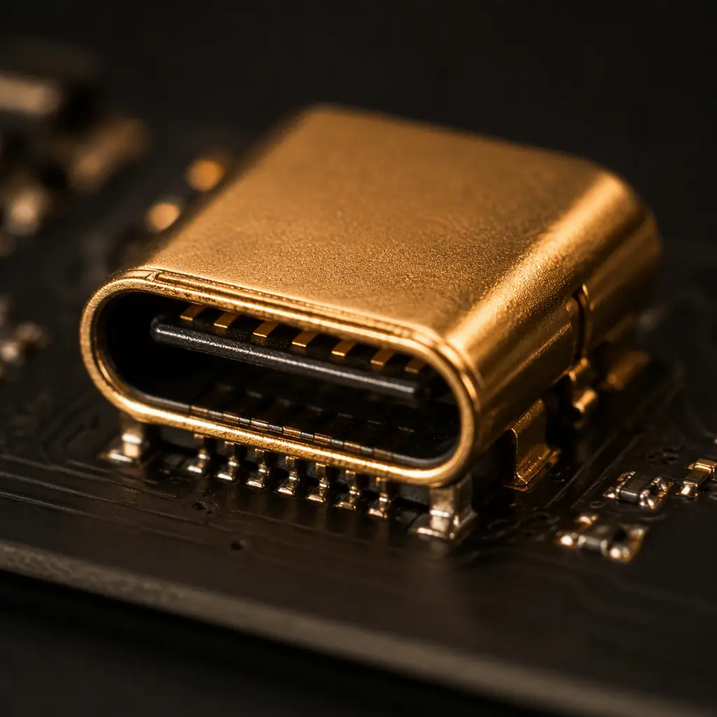
The CC (configuration channel) lines carry the PD protocol signaling and, on 240W designs, the 5A current-advertising; they should be routed as a tightly coupled pair with controlled impedance where the controller datasheet requires it, and kept away from the switching noise of the primary. The D+/D- USB 2.0 pair also benefits from impedance control (90 Ω differential) if the charger supports data. Our USB-C PCB design guide covers the connector and PD routing rules in detail.
Protect the CC/SBU Pins Against ESD and Overvoltage
USB-C connectors see constant plugging and unplugging — the CC pins need ESD protection (a small TVS array) placed within 3-5 mm of the connector, and the VBUS path needs bulk and ceramic capacitance sized for the output ripple spec. For 240W/48V outputs, the VBUS trace must handle 5A continuously: widen it to the copper math in our current capacity guide, and keep the sense lines (if the PD controller does remote sensing) as a clean, separate pair.
Keep the Feedback Path Quiet
The output voltage feedback from the secondary to the primary controller crosses the isolation barrier through an optocoupler or a digital isolator. Route the feedback traces away from the transformer and the switch node, keep the loop area small, and place the compensation components tight to the controller. A noisy feedback path shows up as output ripple and audible noise — two of the most common charger complaints.
Isolation and Safety: Creepage, Clearance, and UL 62368-1
An offline charger has mains voltage (up to 375V peak for 264VAC) on one side of the barrier and user-touchable output on the other. The PCB geometry is a safety device.
Observe the Creepage and Clearance Tables
For reinforced insulation on a 240VAC input with pollution degree 2, IEC 62368-1 requires clearance around 6.0 mm and creepage typically 6.0-8.0 mm between primary and secondary, measured on the actual PCB surface — slots in the board count toward creepage distance, which is why charger boards often have routed slots under the optocoupler. These numbers are the minimums for production; verify against the latest standard and your certifier's interpretation, because they vary with working voltage, altitude, and coating. IPC-2221B gives the analogous board-level guidance. Our UL certification guide explains the process and the UL 94 flammability requirements for the base material.
Use High-Tg, High-CTI Laminate on the Primary
The base material's CTI (comparative tracking index) class determines the creepage distance required: a CTI Class I material (≥600V, e.g., high-Tg FR-4 with ceramic filler) allows shorter creepage than a Class III material. Specify high-Tg FR-4 (Tg 150-170°C) for the whole board — the transformer area gets hot, and low-Tg material degrades and tracks over time. Our PCB materials guide compares the laminate options.
Document the Isolation Design for the Certifier
UL 62368-1 certification requires the certifier to see the isolation distances on the layout, the transformer's isolation construction (margins, triple-insulated wire), and the Y-capacitor ratings. Keep a clean, annotated copy of the layout showing the primary-secondary distances, and make sure the production board matches the certified sample — a last-minute trace reroute across the barrier voids the certificate. The certificate covers the specific board revision; any change to the barrier area needs re-review.
DFM for GaN Chargers: What to Put on the Drawing
A GaN charger board is dense, two-sided, and often assembled with mixed lead-free profiles. Specify these on the fabrication and assembly drawings:
Copper Weight, Via Arrays, and Pad Finishes
State the copper weight per layer (typically 2 oz on power layers), the thermal via arrays under the GaN pad and transformer (diameter, fill/tenting, and whether they are capped), and the surface finish — ENIG for the GaN pads and USB connector, with OSP acceptable on internal power areas. Mismatched via tenting is a common cause of solder voids in the thermal pad.
Panel Design for High-Density Two-Sided Assembly
Charger boards assemble both sides (primary on top, secondary on bottom), so the panelization must survive two passes through reflow. Specify V-score or tab-route panelization with the second-side components inside the panel area, and note the fiducial placement for each side. Our panelization guide covers the layout math.
Test Strategy: Hi-Pot, Load, and EMC Sampling
Production testing for offline chargers is not just functional: every unit gets a hi-pot (dielectric withstand) test between primary and secondary to catch assembly damage to the isolation barrier, plus a load test at rated power. A sample of each batch goes to conducted and radiated EMC verification. Specify the test points and the hi-pot voltage (typically 3000-4000VAC for reinforced insulation at production level) on the drawing. Our testing methods guide places these in the full production strategy.
Summary: The GaN Charger Checklist
A GaN charger that runs cool, passes EMC, and certifies cleanly is designed with a topology matched to the power level, a minimized power loop with tight gate drive, copper sized for current and heat, thermal vias moving heat from every hot component into internal planes, an EMI strategy that starts at the switch node, USB PD pairs routed with impedance control and ESD protection, and primary-secondary isolation that follows the creepage tables exactly. On the production side, hi-pot and load testing on every unit, with EMC sampling per batch, catches the defects that field failures would otherwise find in customers' homes.
At Huaxing PCBA we manufacture GaN chargers and adapters from 20W to 240W+ — 2-8 layers with high-Tg FR-4, 2-6 oz copper, ENIG finishes, laser microvias for the high-density primary side, and full power-supply assembly support: 8 SMT lines, X-ray for the transformer and GaN pads, and hi-pot plus load testing in production. Our DFM review checks the power loop, thermal via arrays, isolation distances, and panelization before tooling. Read our SMPS layout guide for the deeper power-electronics rules, or send your files for a free DFM review and quote.
