
An FPGA board that is electrically correct and still fails at first build is the most demoralising outcome in hardware because there is nothing to fix. The schematic is right, the stackup is right, the decoupling is right, and the board comes back with 40 BGA joints open. The design was never the variable. On large packages, assembly is.
Package body size drives the three failure mechanisms that dominate FPGA assembly: warpage across a 27 to 45 mm body as it passes through the reflow window, paste volume on land pads that shrink faster than the stencil process can follow, and thermal mass mismatch between a heavy package and a thin board that produces a temperature differential across the joint during every profile ramp. Each has numbers attached, and each behaves differently from the fine-pitch QFN experience most engineers have.
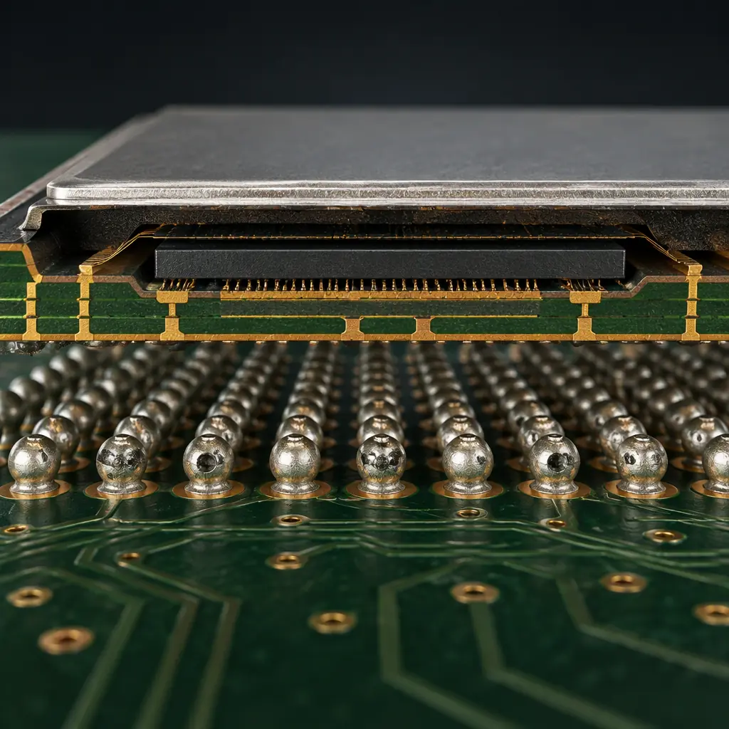
Why an FPGA Package Behaves Differently From a QFN
A QFN warps a little and its joints are peripheral, so the leads comply. A 35 mm BGA cannot comply at all: the die side and the substrate side of the package expand at different rates, the package bows, and the joints at the corners and centre are pulled in opposite directions at the moment the alloy is solidifying. At 0.8 mm pitch the ball has enough volume to absorb some of that motion. At 0.65 mm and below it does not, and the joint either opens, or forms a partial contact that passes the flying probe and fails in the field.
| Package body | Typical ball count | Warpage across reflow window | Dominant risk |
|---|---|---|---|
| 17 to 23 mm | 256 to 484 | 0.05 to 0.10 mm | Paste bridging between pads |
| 27 to 31 mm | 672 to 900 | 0.08 to 0.15 mm | Corner joint open |
| 35 to 42.5 mm | 1,156 to 1,760 | 0.12 to 0.22 mm | Head-in-pillow, centre open |
| 45 mm and above | 2,000 and up | 0.18 to 0.30 mm | Simultaneous corner and centre open, warpage over substrate yield |
The design guidance for stackup, power sequencing and transceiver routing is a separate subject and is covered in the FPGA PCB design guide. Everything below assumes the design was done correctly and asks why it still failed.
The Paste Volume Problem on Large Land Pads
The correct approach for a large BGA land is not the same as for a fine-pitch one. At 0.8 mm pitch the pad is roughly 0.45 mm diameter and the aperture area ratio drives release efficiency; at 0.65 mm the pad drops to about 0.35 mm, and the stencil thickness has to come down to keep the paste from printing as a dome that collapses into bridging during ramp. Below a certain aperture area ratio, paste release becomes inconsistent: some pads get a proper deposit and some get 60% of one, on the same print stroke.
| Pitch | Land diameter | Stencil thickness | Aperture area ratio | Failure signature when wrong |
|---|---|---|---|---|
| 1.0 mm | 0.55 mm | 0.12 to 0.15 mm | Above 0.75 | Bridging on collapse |
| 0.8 mm | 0.45 mm | 0.10 to 0.12 mm | 0.65 to 0.75 | Intermittent open, opened by reflow wicking |
| 0.65 mm | 0.35 mm | 0.08 to 0.10 mm | 0.55 to 0.65 | Partial deposit, head-in-pillow |
| 0.5 mm | 0.28 mm | 0.08 mm, laser cut, nano-coat | Below 0.55 | Unrecoverable without stepped stencil or paste transfer |
Two practical consequences. First, a board carrying both 0.8 mm BGA and 0402 discretes needs either a stepped stencil or a compromise thickness, and the compromise almost always goes against the BGA because the 0402 pads are more forgiving. Second, the paste itself matters: a type 4 or type 5 powder is required below 0.5 mm pitch, and the oxide content of a coarser powder reduces wetting on the small land. The print-side detail of that decision is in the solder paste selection guide.
Thermal Mass Mismatch and the Reflow Window
A 45 mm package with a heat spreader weighs several times what the board under it does. During soak, the package lags the board by 8 to 20°C; during reflow the relationship inverts and the package runs hotter than the thin board at its edges. The joint sees that differential twice per profile, once going up and once coming down, and it is at its most vulnerable during the liquidus and the first seconds of solidification.
The measurements that matter, in the order they should be checked:
Delta-T across the package, not the oven setpoint
A profile that looks correct on a bare coupon will run hot on a populated board with a large thermal-mass package. Thermocouples go under the package edge and at the board centre; the target is a delta of 5°C or less through the liquidus, and if it cannot be achieved, the soak has to be lengthened rather than the peak raised.
Time above liquidus versus warpage
Longer time above liquidus improves wetting and worsens warpage, because the package is bowed for longer while the joint is molten. For a package above 35 mm this trade-off usually lands at 50 to 70 seconds above liquidus with SAC305, not the 90 seconds that works well on fine-pitch QFPs.
Cooling rate through solidification
Fast cooling produces a finer grain structure and better joint strength, but on a large package it also freezes the warpage in place, because the package is still bowed when the alloy becomes solid. The usual compromise is 2 to 4°C per second, applied uniformly with real forced convection rather than the oven's nominal setting.
Void and Head-in-Pillow Rates by Alloy
The void rate on a large BGA is a property of the paste chemistry and the profile together, not of the equipment alone. The numbers below are typical for a 35 mm package and are the ranges we plan against:
| Paste system | Typical void area at 35 mm body | Head-in-pillow risk | When it is the right choice |
|---|---|---|---|
| SAC305 type 4, no-clean | 8 to 18% | Moderate | Default for industrial and telecom boards |
| SAC305 type 4, water-wash | 5 to 12% | Low | Where cleaning is available and ionic contamination matters |
| Low-temperature SnBi, type 4 | 15 to 25% | High | Only where the package cannot survive 245°C, and then with a warpage plan |
| SAC305 with vacuum reflow assist | 2 to 6% | Low | High-reliability FPGA boards where an open is unacceptable |
The IPC-7095 accept criteria are what decide whether a given void rate is a reject or a pass, and they are class and application dependent. The working version of that table, including how to measure void area from an X-ray slice, is in solder voiding X-ray acceptance criteria. Head-in-pillow is the specific failure where the ball sits on an oxide layer instead of having coalesced, looks electrically connected at low current, and opens under thermal cycling; the mechanism and its signature are covered in head-in-pillow BGA defect.
Board Warpage Is Now a Design Variable
Half the warpage problem is the package. The other half is the board, and that half is under the designer's control. A 0.8 mm board carrying a 45 mm package with asymmetric copper distribution will bow during reflow on its own, independent of the package. Thickness, copper balance and stiffener placement set how much.
| Board thickness | Copper balance | Expected board warpage over 45 mm | Verdict |
|---|---|---|---|
| 0.8 mm | Asymmetric | 0.15 to 0.25 mm | Unbuildable with a large BGA |
| 1.6 mm | Asymmetric | 0.06 to 0.12 mm | Marginal, needs fixture support |
| 1.6 mm | Balanced within 10% | 0.03 to 0.07 mm | Acceptable |
| 2.0 mm or stiffened | Balanced | Under 0.03 mm | Preferred for 45 mm and above |
The design measures that manage it, from the substrate side rather than the package side, are set out in PCB warpage and BGA assembly. The short version: balance copper by layer, keep the package centre over a continuous plane, and if the board must be thin, put the stiffener in the mechanical design rather than hoping the fixture compensates.
The First-Article Report to Demand
A first-article inspection that reports dimensional conformance on a bare board tells you nothing about whether the BGA attached. The report for a large FPGA board should contain the following, and a supplier who cannot produce it has not built one before:
BGA X-ray with void percentage per ball, corner and centre reported separately
A single average void figure hides exactly the region that fails. Corners and centre must be reported as separate populations against IPC-7095 limits for the class.
Real thermal profile from the populated board, with the thermocouple locations named
Under the package edge, at the package centre, and at a bare board location as reference. A profile from a test coupon is not evidence.
Cross-section of at least three balls, one corner, one edge, one centre
The microsection is where head-in-pillow is visible. Its signature and how to read it are in the microsection analysis guide.
Board warpage measurement before and after reflow
Measured on the assembled board at room temperature, using a defined support and measurement method. Post-reflow warpage above 0.1 mm over the package footprint predicts early field failures.
Boundary-scan or JTAG interconnect test result
If the chain was designed in, the interconnect test is the only cheap way to prove every package ball connects. Its result belongs in the first-article package, not in a separate document nobody reads. The general method is in PCB design for testability.
Frequently Asked Questions
Why does a large FPGA BGA fail when the same design rules worked on a smaller package? Because the failure mechanisms scale with body size. Warpage roughly doubles from a 23 mm to a 45 mm body, and the joint compliance that absorbed it at 0.8 mm pitch is reduced at 0.65 mm. The rules are not wrong, they are incomplete above roughly 35 mm.
Is low-temperature paste a fix for warpage? It reduces the peak temperature, which helps a temperature-sensitive package, but SnBi alloys are more brittle and void more. It is the right choice when the package cannot survive 245°C, and the wrong choice when the problem is warpage, because the joint still freezes while the package is bowed.
How much void is acceptable? For a Class 2 industrial board, up to 25% void area per ball is commonly accepted with no single void over a defined diameter; for Class 3 and high-reliability, the limits tighten substantially. The full criteria and how to measure them are in X-ray acceptance criteria.
Can a large BGA be reworked? Yes, with a dedicated rework station and a preheat plan, but the second reflow cycle worsens warpage and the joint quality of the reworked region is measurably worse than the original. On boards where more than a few packages need rework, the process is the problem, not the individual unit.
What board thickness should a 45 mm package sit on? 1.6 mm with copper balanced within 10% is the minimum, and 2.0 mm or a stiffened design is preferred. On 0.8 mm, the board's own warpage exceeds the joint's tolerance regardless of how good the package is.
Build the First Article Before the Volume Order
Send the Gerber, the stackup and the package land pattern. We return a first-article plan written against your package size: the reflow window with thermocouple locations, the stencil thickness and paste type, the X-ray accept criteria and the void reporting format, and the warpage measurement method. If the design cannot hit the target on the current stackup, we say so before a single board is built, rather than after the first 200 fail.