
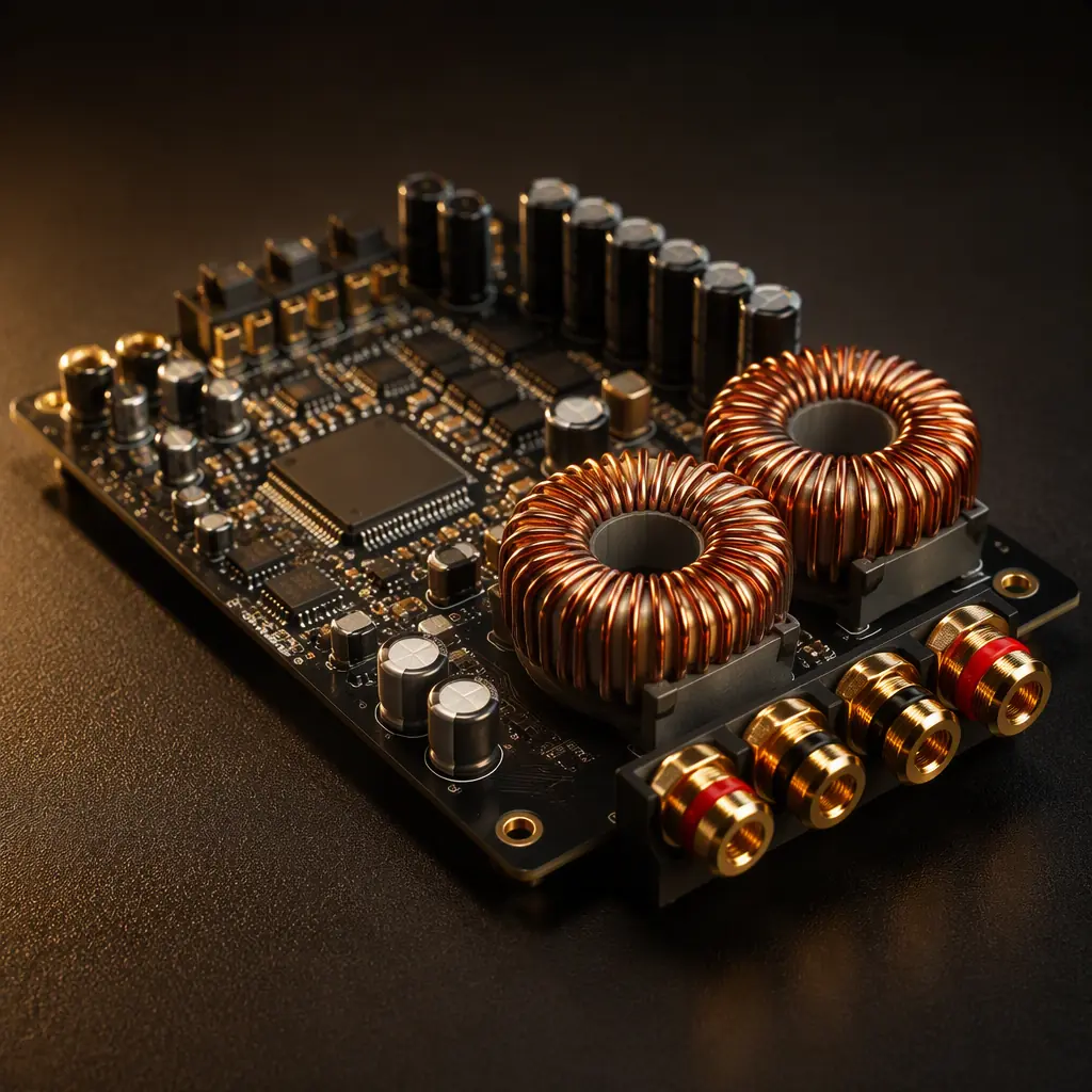
Class-D amplifiers now dominate everything from 3W smart-speaker drivers to 2000W subwoofer modules, for one reason: efficiency. A class-AB amp wastes 40-50% of the supply power as heat, while a well-designed class-D stage converts 85-92% of the input power into speaker output. That difference is why battery-powered Bluetooth speakers can run for a day, why automotive amplifiers fit behind a dashboard, and why a 100W-per-channel home theater receiver no longer needs a giant heatsink. The cost is complexity: a class-D amp is a switching power stage switching at 300 kHz to 1.2 MHz right next to a high-gain analog audio path, and the PCB is where those two worlds collide.
Huaxing PCBA manufactures amplifier boards for consumer audio, automotive infotainment, and professional PA equipment — 2-8 layer stackups with 2-6 oz copper on power layers, ENIG finishes for the amplifier ICs, X-ray inspection for high-density power stages, and full functional and audio test support. This guide covers the power stage layout, output filter design, ground and noise discipline, thermal management, EMC, and the DFM specifications to put on the drawing.
How Class-D Works — and What the PCB Must Do
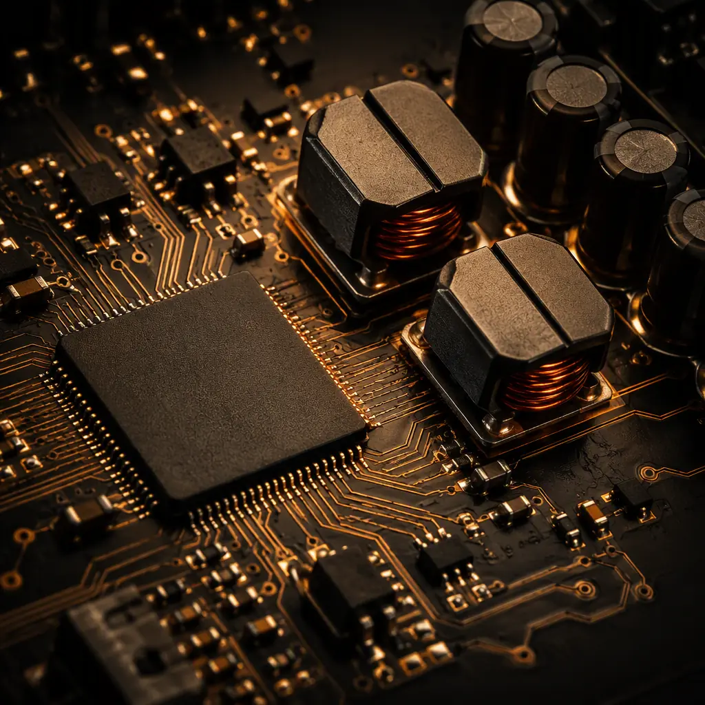
A class-D amplifier converts the audio signal into a high-frequency pulse-width-modulated square wave, amplifies that square wave in a half-bridge switching stage, then reconstructs the audio with a low-pass LC filter at the output. The switching frequency is typically 384 kHz to 768 kHz (with spread-spectrum modulation on modern controllers to spread the EMI), well above the 20 kHz audio band.
The Board Carries Two Conflicting Worlds
The power stage is a fast switcher: 20-40V rails (or ±35V for higher-power designs), switching currents in the amps, and edges in the low-nanosecond range. The input stage is a high-gain analog circuit that amplifies millivolt audio signals by 20-30 dB. The layout's job is to keep the switcher's noise out of the analog path while giving the power stage the tight loops it needs. This is the same discipline our mixed-signal PCB design guide describes, applied to power audio.
Every dB of Noise Has a Physical Source
Output noise in a class-D amp comes from specific places: switching ripple leaking past the output filter, ground bounce from the power stage's return currents, coupling from the switch node into the input stage, and the controller's own PWM jitter. Each of these is a layout problem with a layout fix. A design that measures -100 dB noise and one that measures -70 dB differ mostly in how the power and analog sections are placed, grounded, and separated.
Efficiency Claims Only Hold With Good Layout
The datasheet efficiency curve assumes a minimum loop inductance and gate-drive path. A sloppy layout adds switching loss at every edge, raises the FET temperature, and can trigger the over-current or over-temperature protection earlier than the design intends. The thermal and the electrical design are the same layout.
Key Takeaway: Class-D is a power converter and a precision audio circuit on one board. Every layout decision — loop size, ground scheme, filter placement — serves both masters, and the compromises are where noise comes from.
The Power Stage: Half-Bridge, Gate Drive, and Switching Loop
Most designs use an integrated class-D controller with built-in gate drivers (TI TAS/TPA series, Infineon MERUS, ST, or NXP parts), driving external MOSFETs for high power or integrated FETs for low power. The layout rules below apply to both.
Minimize the Half-Bridge Switching Loop
The loop formed by the high-side FET, low-side FET, and the local bulk capacitor across the supply rails carries the full switching current. Keep it small — a tight cluster on one side of the board with the capacitor physically adjacent to the FETs, connected by short wide traces or a dedicated copper pour. Loop inductance here causes voltage overshoot at the switch node, increases EMI, and wastes efficiency. A loop area under 1 cm² is a practical target for a 100W channel. Our SMPS layout guide covers the same loop-minimization physics in detail.
Route the Gate Drive as a Tight, Separate Pair
The gate drive trace from the controller to each FET's gate must be short (under 10 mm where possible) and run as a tight pair with its return path, away from the switch node and the output traces. Add the gate resistor right at the FET gate. A long or noisy gate trace makes the FET switch slower or oscillate — slow switching burns efficiency, oscillation burns the FET. If the controller and FETs are in one package, this is handled internally and the layout effort moves to the output filter and supplies.
Size the Supply and Output Copper for Peak Current
A 100W channel into 4Ω draws about 5A RMS from the supply, with peaks near 10A. The supply traces, the output traces to the filter, and the speaker output must be sized for that current with margin — 2 oz copper minimum on the power path, wider where the traces are long. Voltage drop in the supply path sags the rails under bass transients, which is audible as compression. Use the copper math in our current capacity guide rather than guessing.
Key Takeaway: The switching loop and the gate drive are the two sacred geometries of a class-D power stage: one as small as possible, the other as clean as possible. Everything else follows.
The Output Filter: Inductors, Capacitors, and Placement
The LC filter between the switch node and the speaker reconstructs the audio and — critically — shapes the EMI. Its layout is as important as its values.
Choose Inductors Rated for the Real Current
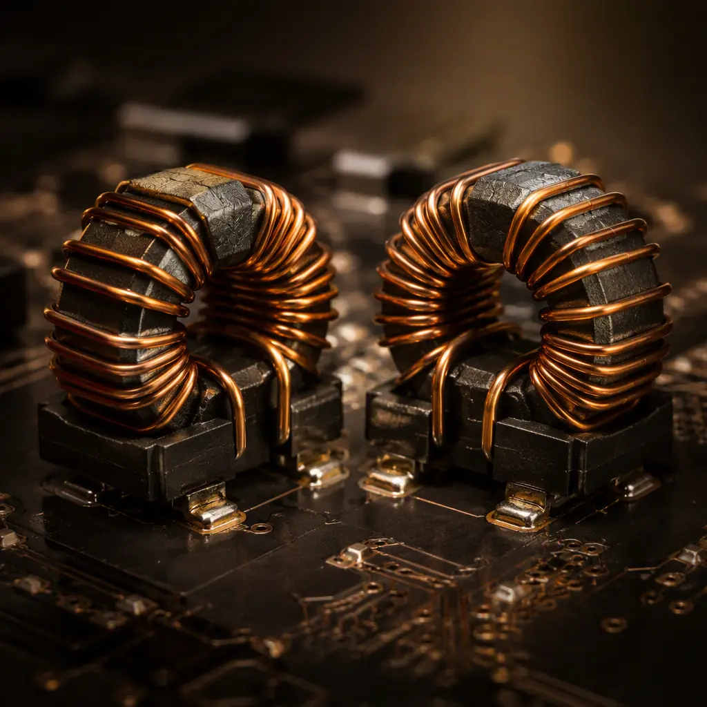
Output filter inductors carry the full speaker current plus the switching ripple. A 10-22 µH ferrite inductor with a saturation rating well above the peak current is typical; running the inductor into saturation collapses the filter and dumps switching spikes into the speaker. Check the saturation curve at the operating temperature, not just the datasheet headline number. Metal-alloy or high-saturation ferrite cores are standard for 100W+ channels. The inductor's DC resistance also matters: 100 mΩ costs about 0.5W of heat at 5A.
Place the Filter Close to the Switch Node, Keep the Path Short
The trace from the switch node to the inductor, and from the inductor to the filter capacitor and speaker terminal, should be short and wide. The filter capacitor (typically 0.47-1 µF film or C0G ceramic, plus a snubber) sits between the inductor output and ground, with its ground returned directly to the power ground plane. Long, thin filter traces add inductance that turns the filter into a resonant antenna. Keep the speaker output pair (plus and minus) as a twisted or tightly-coupled pair to the connector.
Add a Zobel Network and Snubber Per Datasheet
Most class-D reference designs specify a Zobel network (typically 10Ω + 100 nF) at the speaker output to keep the filter stable with reactive loads, and an RC snubber across the switch node to damp ringing. Place these physically at the points they protect — the snubber right at the switch node, the Zobel right at the speaker connector. Component placement here is part of the circuit, not decoration.
Grounding and Noise Discipline: Keeping the Audio Clean
The difference between a good amplifier and a noisy one is almost always the ground scheme. Class-D controllers use separate power ground and analog ground (AGND) pins precisely so the layout can keep the two apart.
Use a Star or Single-Point Ground Between Power and Analog
Connect the power ground (return path for the switching current) and the analog ground (input stage, feedback, controller's analog section) at exactly one point — usually a star point near the controller or at the input connector ground. The switching return current must never flow through the analog ground plane. Split the ground pour if needed to enforce this, and bridge the split only at the star point. Our mixed-signal grounding guide explains the theory in depth.
Keep the Input Stage Physically Opposite the Power Stage
Place the audio input connector, input filter, and the controller's analog input pins at the board edge farthest from the switching stage and the output filter. Do not route the input traces across or under the power section on any layer. If the board is long, treat the middle as a buffer zone with the ground plane intact but no signal routing. Shielding the input stage with a grounded guard trace around the input traces is cheap insurance on high-gain designs.
Filter the Supply Rails at Every Stage
The amplifier's supply pins need local decoupling: bulk electrolytic (470-2200 µF per channel, placed near the power stage) plus ceramic caps (100 nF and 10 µF) right at the controller and FET supply pins. The analog supply for the input stage gets its own LC or RC filter, fed from the main rail with a ferrite bead. This keeps the PWM current ripple from modulating the analog supply — a classic cause of audible buzz. Our power integrity guide covers the decoupling methodology.
Key Takeaway: Noise in class-D is a ground problem before it is anything else. One star point, separate power and analog grounds, physical separation of input and output stages, and filtered supply rails eliminate most audible artifacts without changing a single schematic value.
Thermal Design for 100W+ Channels
Even at 90% efficiency, a 100W channel dissipates 10W, and a 4-channel amp dissipates 40W. The PCB must move that heat out.
Give the FETs and Controller a Real Thermal Path
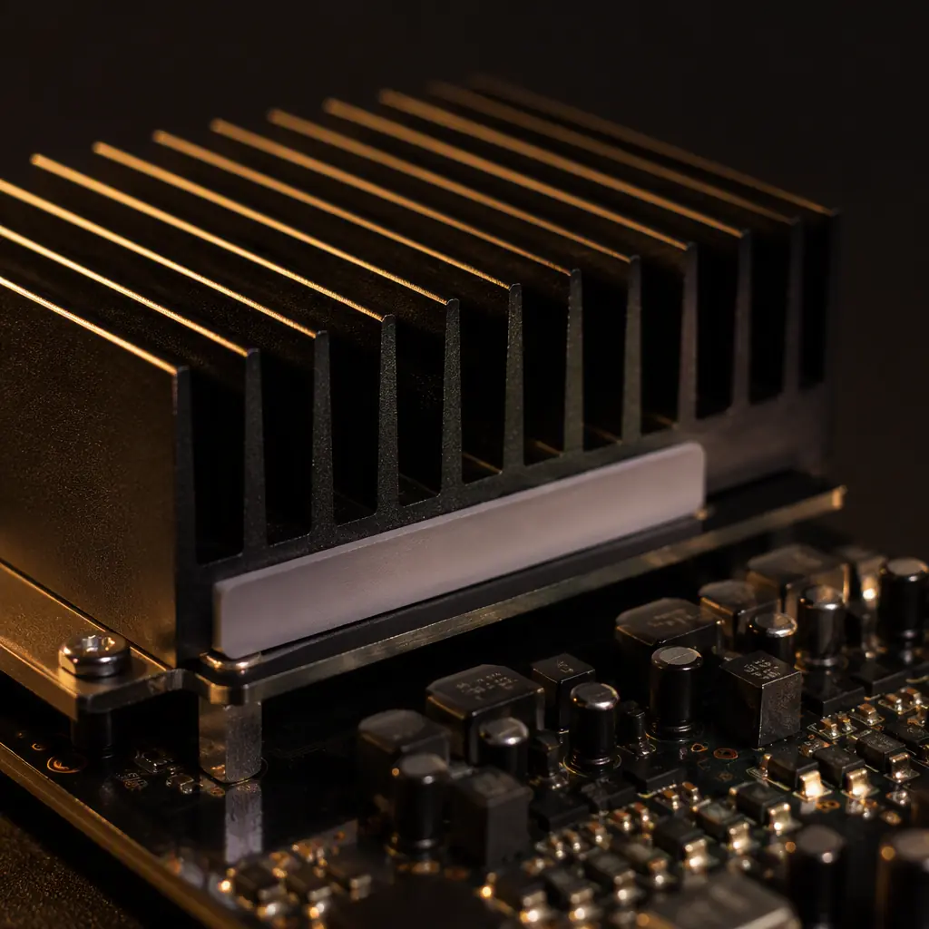
The output FETs (or the integrated amp package) expose a thermal pad that must connect through a via array to a copper pour that covers as much board area as the layer budget allows. Use 10-25 thermal vias (0.3 mm, tented or filled) under the pad, tie them to a continuous pour on layers 2 and 3, and connect that pour to the enclosure heatsink with a thermal pad or to the board edge for airflow. Do not route signal traces through the thermal pour — keep it a clean heat spreader. Our thermal management guide details the via and pour design.
Spread the Channels and the Heat
On multi-channel boards, distribute the channels across the board rather than clustering them, so each channel's copper area contributes to cooling the others' heat. Keep the electrolytic capacitors away from the FETs and the output inductors — their lifetime halves for every 10°C rise. The output inductors and the rectifier/freewheeling diodes are secondary heat sources that still need airflow or copper.
Verify With a Full-Power Load Test
Run the prototype at full rated power into a resistive load (4Ω and 8Ω) with continuous sine or pink noise for 30+ minutes, and measure case and component temperatures. The thermal test is also the stability test — a marginal loop that oscillates at high temperature shows up here first. Document the thermal images; they are the evidence your enclosure designer needs. Our thermal cycling testing guide covers the long-term reliability angle.
EMC: Switching Noise vs. FCC Part 15B / CISPR 32
A 768 kHz switcher driving 5A into a speaker cable is a textbook radiator. Class-D amps must pass FCC Part 15B (US) or CISPR 32 / EN 55032 (EU) for consumer equipment — and the speaker cable is usually the biggest antenna in the system.
Use Spread-Spectrum Modulation and a Clean Switch Node
Modern class-D controllers offer spread-spectrum PWM that dithers the switching frequency, spreading the emission energy so it falls under the quasi-peak limits. Enable it by default. Pair it with a physically small switch node (minimal copper area, tight loop) and a well-placed snubber, and most radiated problems disappear before the filter stage. Our EMI/EMC design guide covers the general methodology.
Add a Common-Mode Choke on the Speaker Output
The speaker cable is a long antenna driven by the amplifier output. A small common-mode choke (or ferrite beads) on the output pair suppresses the common-mode current without affecting the differential audio — this is the single most effective EMC fix on class-D boards. Place it right at the speaker connector, with the filter ground returned to the power ground star point. Also route the input cable's ground carefully: a ground loop through the input cable is a classic cause of both hum and failed radiated tests.
Plan the Compliance Test Early
Run a pre-compliance radiated scan at the prototype stage — a desktop spectrum analyzer with a near-field probe finds the hot spots (switch node, inductor, speaker connector) in minutes. Fixing EMI at the prototype costs a trace reroute; fixing it at the certification stage costs a board respin and weeks of delay. Budget for the scan in every class-D project.
DFM for Amplifier Boards: What to Put on the Drawing
Amplifier boards combine high-current copper, mixed SMT/through-hole parts, and often thick copper pours that need special fab attention.
Specify Copper Weight, Finish, and Thermal Vias
State the copper weight per layer (2 oz minimum on power layers, up to 6 oz for very high-current designs), the surface finish (ENIG for the amplifier IC pads and connector areas), and the thermal via arrays under the FETs and amp ICs — diameter, fill, and whether the vias are capped for soldering. Unspecified thermal vias get made however the fab defaults, which is how thermal pads end up with voids.
Mixed Assembly: SMT + Through-Hole Power Parts
Speaker terminals, supply connectors, and large electrolytics are through-hole, while the controller and FETs are SMT. Plan the assembly order: SMT first, then through-hole, with wave or selective soldering for the THT side. Note any press-fit or screw-terminal requirements on the assembly drawing. Our SMT vs through-hole comparison and wave vs selective soldering guide cover the process trade-offs.
Test Strategy: Audio and Power on Every Unit
Production testing for amplifiers needs more than a power-on check: a functional audio test (output at 1 kHz, THD+N measurement, and DC offset check on every unit) plus a soak test at partial power catches assembly defects — wrong filter parts, reversed FETs, cold joints on the power path — that a visual inspection misses. Specify the test points and the test jig requirements on the drawing. Our testing methods guide places audio functional test in the full production strategy.
Summary: The Class-D Amplifier Checklist
A class-D amplifier that delivers rated power, runs cool, sounds clean, and passes EMC is designed with a minimized switching loop, a clean gate drive, filter inductors rated for real current and placed tight to the switch node, a single-point ground scheme that keeps switching current out of the analog path, physical separation of input and power sections, a real thermal path from every hot device into the board, and a production test that measures audio quality on every unit. The schematic gives you the circuit; the layout gives you the amplifier.
At Huaxing PCBA we manufacture class-D amplifier boards from 3W portable drivers to 1000W+ pro-audio modules — 2-8 layers with 2-6 oz copper, ENIG finishes, thermal via arrays, mixed SMT/through-hole assembly on 8 SMT lines plus 4 DIP lines, and functional audio test support in production. Our DFM review checks the power loops, thermal vias, ground scheme, and assembly order before tooling. Read our audio & HiFi PCB manufacturing guide for the material and cleanliness side of audio boards, or send your files for a free DFM review and quote.
