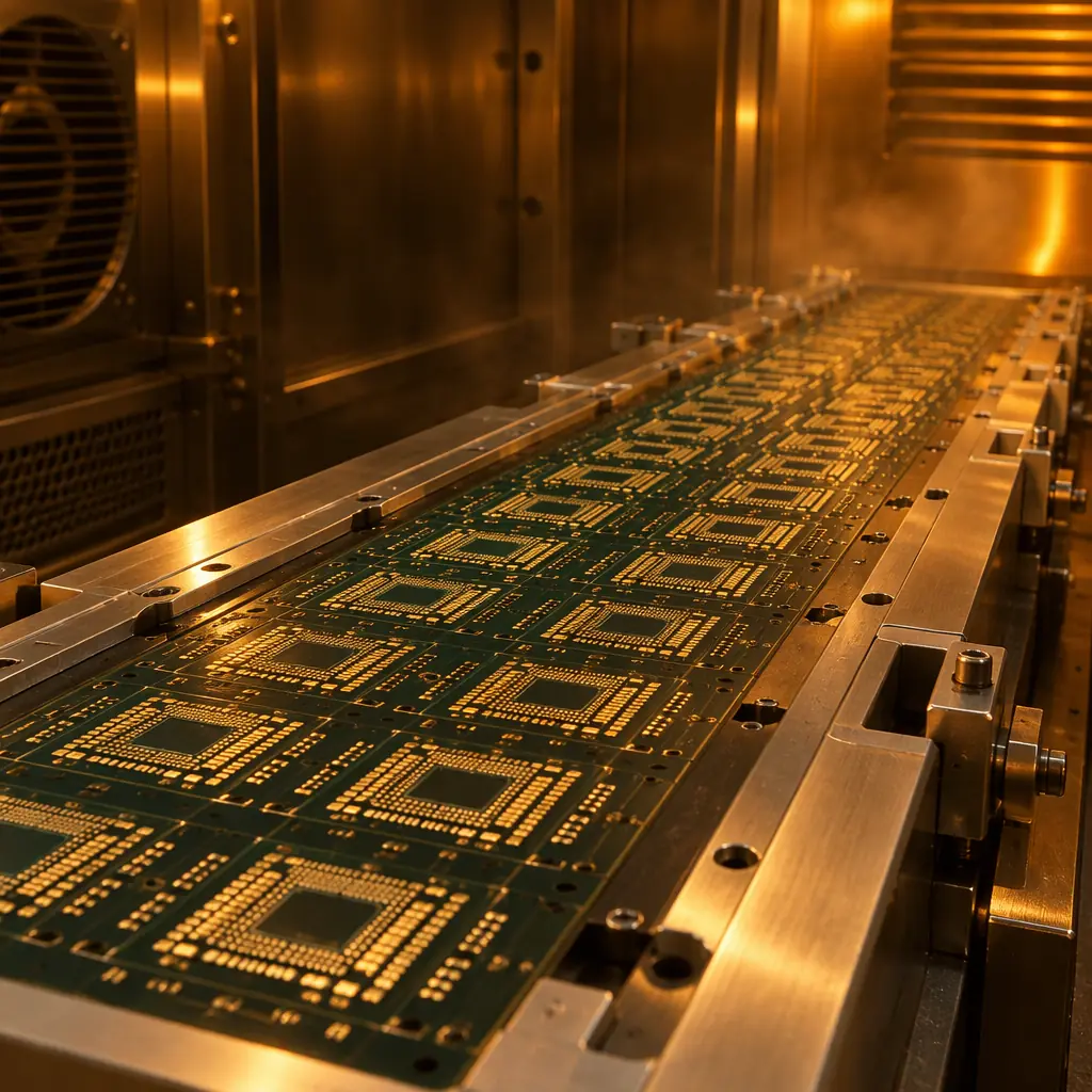
A burn-in board is the only PCB in a semiconductor test flow that is asked to survive hundreds of thermal cycles, continuous electrical bias, and repeated mechanical insertion, while proving that the device under test is good rather than proving anything about itself. That last part is what makes the requirements unusual. A functional test board that degrades quietly will report a failure that belongs to the board, not to the part, and the failure will be logged against a device lot that was in fact fine.
Most specifications for these boards are written by copying a previous program. This article covers what the board actually has to survive, why the failure usually appears at the pad rather than at the solder joint, and which parameters to put on the drawing so the board can be bought against a number instead of a habit.
What a Burn-In Board Has to Survive
Three loads act on the board simultaneously and they interact. The thermal load is a chamber cycle, typically from ambient to a soak between 125°C and 150°C and back, repeated for the duration of the burn-in run and then across the board's own life of many runs. The electrical load is continuous bias applied through the board to every device position, often at elevated voltage and current, which means continuous Joule heating in the power distribution and continuous electrochemical stress wherever moisture and ionic residue meet a biased surface. The mechanical load is the insertion cycle: every device position is loaded and unloaded at every run, and every contact in the socket assembly pushes against a pad on the board.
Thermal: Continuous Soak, Not Just Cycling
A burn-in board spends the majority of its life at soak temperature with bias applied, not in transition. That changes the material requirement from thermal shock resistance to long-term thermal stability under voltage. The laminate property that matters most is not the glass transition temperature alone but the decomposition temperature and the long-term thermal ageing behaviour at the soak temperature plus margin. A laminate rated at a Tg just above the soak temperature is operating with almost no margin, and its Z-axis expansion at soak will fatigue the plated barrels over the board's run count.
Electrical: Bias Plus Moisture Is the Corrosion Engine
Continuous DC bias on an insulated surface with any ionic contamination present produces electrochemical migration. The failure looks like a leakage path or a dendritic short between adjacent features, and it appears after weeks of operation rather than at first test. Two controls matter: cleanliness at a defined ionic contamination level measured on the finished board, and a solder mask and surface finish system that does not provide a moisture path between biased conductors. A conformal coat is not a substitute for cleanliness on a board that will be handled and reinserted hundreds of times.
Mechanical: The Insertion Cycle Is the Wear Mechanism
Every burn-in run applies a defined normal force per contact across every device position. Over hundreds of insertions the cumulative effect is abrasive wear at the contact pad, and the pad's ability to survive that wear is a function of the finish, not the laminate. This is why board life is usually limited by contact pad wear rather than by any electrical or thermal parameter: the board is electrically perfect and mechanically worn out.
Key Takeaway: Specify a burn-in board against the three loads it will actually see, with the number of insertion cycles and the soak temperature on the drawing. A specification that lists layer count and laminate without the run count and the soak temperature has not described the product.
Laminate Selection Under Continuous Bias at Temperature
The dominant laminate question is not whether the material survives one trip to 150°C, which most high-Tg FR-4 will do, but whether it holds mechanical and electrical properties across the board's service life at that temperature with bias applied. Three properties drive the decision.
| Property | Why it matters on a burn-in board | Practical specification approach |
|---|---|---|
| Decomposition temperature | Governs mass loss and outgassing at soak; low Td material degrades cumulatively across runs | Specify Td with a stated margin above soak temperature, measured by TGA at 5% mass loss |
| Z-axis CTE above Tg | Drives barrel fatigue in through-hole and socket vias as the board cycles | Request Z-axis expansion data across the operating range, not a single CTE number |
| T260 and thermal stress | Indicates the laminate's ability to survive repeated assembly and rework excursions | State the rework expectation; a board that will be reworked needs T260 evidence |
| Dielectric loss and insulation resistance at temperature | Bias leakage changes with temperature; insulation resistance at soak affects measurement validity | Request insulation resistance at soak temperature, not at room ambient |
| CTE match to the socket body | Mismatch loads the contact interface as the assembly heats | State the socket material and its CTE; require the stackup to be reviewed against it |
The CTE match row is often overlooked because the board is specified in isolation from the socket that will be mounted on it. A socket body with a significantly different expansion coefficient will move relative to the board at soak temperature, and the contact interface absorbs that movement on every cycle. On a large board with many sockets, the cumulative movement across the board diagonal is not negligible, and it shows up as intermittent contact at the outermost positions before it shows up anywhere else.
Pad Finish: The Real Wear-Out Part
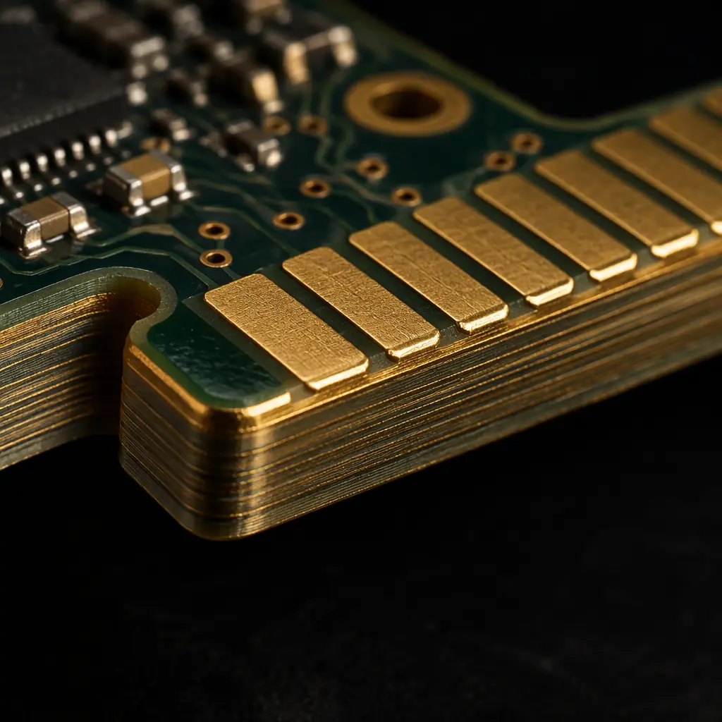
Contact pads on a test board wear by abrasion, and the finish determines how many cycles they survive. Hard gold over nickel is the standard answer for a reason: the gold provides a low and stable contact resistance and does not oxidise, and the nickel layer beneath provides a hard substrate that resists the contact's penetration. The variables that matter are gold thickness, nickel thickness, the gold's hardness and purity, and whether the nickel barrier is continuous.
Thin gold is the most common specification error. A flash of gold over nickel that measures a fraction of a micron at the contact face will be penetrated by the contact's wear track within a modest number of insertions, exposing nickel, which oxidises and raises contact resistance. The specification should state a minimum gold thickness at the contact area after plating, with the measurement method and the location, because the thickness at the contact face is what governs life and the thickness at the panel edge is not a proxy for it.
State Insertion Cycles and Derive the Finish From It
The drawing should state the required insertion cycle count, and the finish specification should be justified against it with the supplier's wear data. A board that will see fifty cycles and a board that will see five hundred are different products, and the difference is expressed in gold thickness and surface hardness, not in layer count.
The Nickel Barrier Must Be Continuous Over Copper
Gold over copper without a nickel barrier diffuses, and the resulting contact resistance drifts with temperature and cycles. The specification should require the nickel layer with a stated minimum thickness and should require the plating sequence to be verified by cross-section on the first article, not assumed from the process tank schedule. Our PCB cross-section report guide covers what a usable plating stack measurement looks like.
Contact Geometry Drives Local Pressure
The pad's size and shape relative to the contact's wear track determines contact pressure per unit area. A pad much narrower than the wear track will show edge wear first and will fail at the ends. The socket vendor's recommended land pattern should be used unchanged; a pad modified for routing convenience changes the pressure distribution and shortens life.
Fine-Pitch Escape on Device Sockets
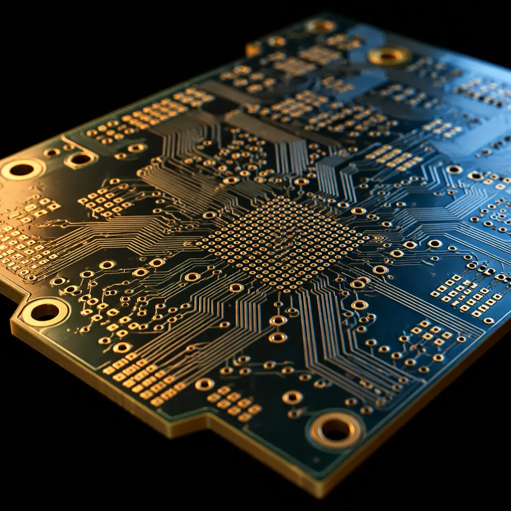
Modern device packages with 0.4mm and 0.35mm pitch force the escape routing on the board into a very small area. The constraint is not the trace width, which can be made small, but the combination of via diameter, via-to-pad clearance, and the number of signal layers available after the ground and power planes. A typical 0.4mm pitch array needs a via-in-pad design with filled and capped vias, or a multi-layer escape with staggered microvias.
On a burn-in board the escape has an extra constraint that a product board does not: the region under the socket is subject to the same thermal and mechanical load as the contact area, and it cannot be underfilled or encapsulated because the socket must remain serviceable. A via-in-pad that is filled and capped but not planar will hold the socket off the board by a few tens of microns, which changes the contact force at every position. Planarity, not just fill, is a specification item.
Count the Layers From the Escape, Then Add Planes
Start with the number of signal layers the escape requires at the specified pitch and pad geometry, then add power and ground layers, then add layers for the routing between device positions. Boards specified by copying a previous layer count usually turn out to be one or two layers short, and the shortage is discovered as a routing compromise under the socket rather than as a decision.
Via Fill and Cap Planarity Needs a Number
Specify the maximum dimple or protrusion at the filled via surface with a measurement method. "Filled and capped" without a planarity limit allows a dimple that the socket's contact will read as an uneven surface. Our PCB via technology guide covers the fill and cap options and their dimensional characteristics.
Impedance and Crosstalk on Bias Lines
Bias lines carrying switching current into a device position both radiate and receive. Adjacent positions on a dense board couple, and the coupling produces measurement artefacts that read as device failures. A ground plane under the bias distribution and spacing of the highest-current lines away from sense lines is a layout rule, but it has to be stated, because the routing pressure at fine pitch tends to consume it first. Our impedance control guide covers controlled-impedance structures on high-layer-count boards.
What to Specify on the Drawing
A burn-in or load board drawing that can be bought against has the following items stated numerically. Anything left to "supplier standard" will be decided by whoever quotes lowest.
| Drawing item | What to state |
|---|---|
| Soak temperature and duration per run | Temperature, dwell, number of runs expected over board life |
| Insertion cycle requirement | Total cycles over life, with the contact type and normal force per contact |
| Stackup | Layer count, laminate family with Td and Tg evidence, Z-axis expansion data, copper weights |
| Contact pad finish | Nickel thickness minimum, gold thickness minimum at contact face, hardness, measurement location |
| Device land pattern | Socket vendor part number and land pattern revision, used without modification |
| Via treatment under sockets | Fill and cap requirement with planarity limit and measurement method |
| Cleanliness | Ionic contamination limit with test method, measured on finished board |
| Warpage | Maximum bow and twist as a percentage, measured at the socket mounting span |
| Traceability | Lot identification method, material certificate retention, per-board serialisation if required |
| Acceptance standard | Class and standard for the bare board and, separately, for the assembled board |
The warpage item is specific to this product class. A burn-in board populated with many sockets will not sit flat if it bows, and a bowed board loads the outer socket positions differently from the centre. Warpage measured over the full board diagonal is not the right measurement; it should be measured across the span between the first and last socket, which is where the flatness actually matters.
Summary: Buy Against the Run Count
Burn-in and load boards fail in ways that look like device failures, which is why their specification deserves more attention than it usually gets. The laminate has to hold its properties across a life spent at soak temperature under bias. The contact finish has to survive the insertion cycles the program will actually run. The escape under the socket has to be dimensional, not just routed. And all three have to be stated as numbers on the drawing so that the board can be bought against them.
At Huaxing PCBA we build test and burn-in boards on high-Tg laminates up to 58 layers, with controlled-impedance coupons on every panel, hard gold contact finishes specified to thickness at the contact face, via fill and cap planarity verified by cross-section on the first article, and ionic contamination measured on the finished board. Our probe card and ATE fixture design guide covers the wafer-probe side of the same flow, and our burn-in and environmental stress screening guide covers what happens to the devices once they are in the chamber. Contact our engineering team with your socket part number and run count for a stackup review.