

Capabilities / PCBA Assembly / SMT
Eight Yamaha and ASM high-speed SMT lines running 24/6 at our Shenzhen factory. From 0201 chip components to 55mm BGAs: every placement is verified in real time with vision alignment and post-reflow 3D AOI.
SMT Core Capabilities
0201 (0.6x0.3mm) passives through 55x55mm BGAs. QFNs down to 0.3mm pitch, QFPs, CSPs, LGAs, and connectors. Dual-lane placement handles mixed component sizes in a single pass, no secondary placement step required.
Yamaha YSM20WR fine-pitch placers achieve ±15µm placement accuracy at 3σ. Vision alignment with 8-camera system verifies every component before placement. Automatic offset correction compensates for board stretch.
Combined output of over 8 million placements per day across all lines. Automatic changeover under 3 minutes between batches. Suitable for both high-mix low-volume prototyping and 100K+ mass production runs with consistent quality.
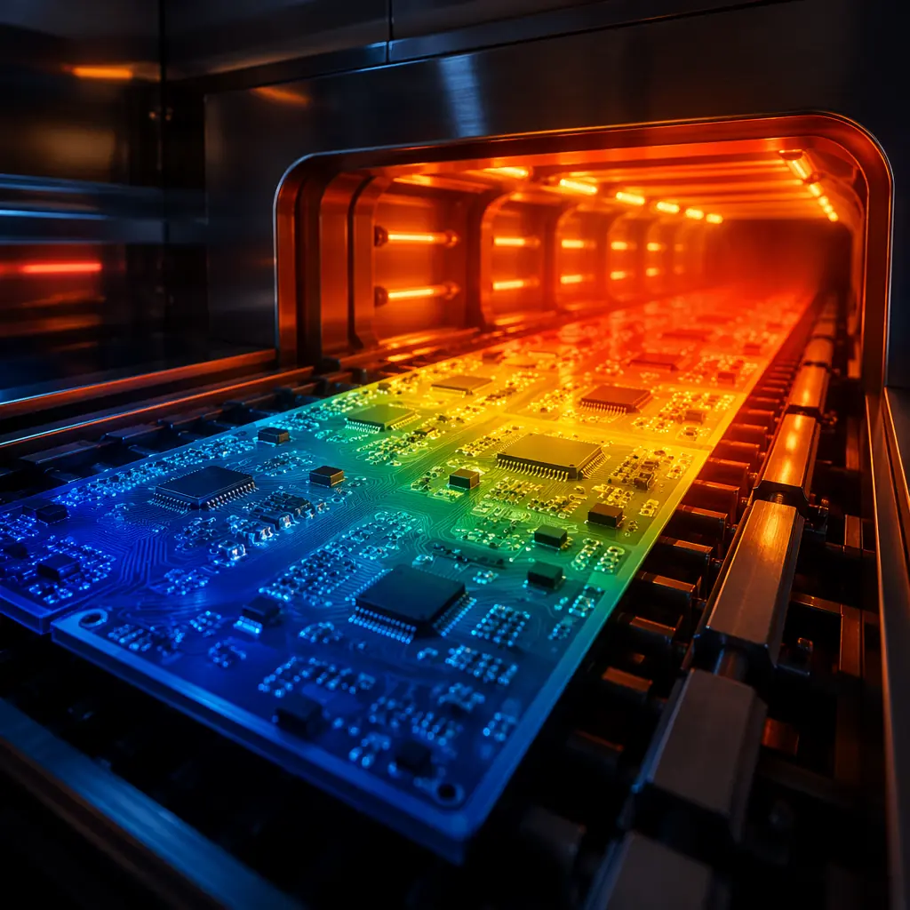
All 10-zone reflow ovens run nitrogen atmosphere as standard. Oxygen levels below 500 ppm. Result: brighter solder joints, reduced voiding, better wetting on fine-pitch and BGA packages. No oxidation-related defects.
IPC-A-610 Class 2 as baseline for commercial/industrial products. Class 3 for automotive, medical, and aerospace, tighter acceptance criteria on solder fillet, void percentage, and joint geometry. IPC J-STD-001 soldering processes.
Pre-production DFM review included with every order. We validate footprint-to-package match, stencil aperture design, component spacing per IPC-7351, polarity/orientation, and BOM completeness before any material is loaded.
Process Step 1
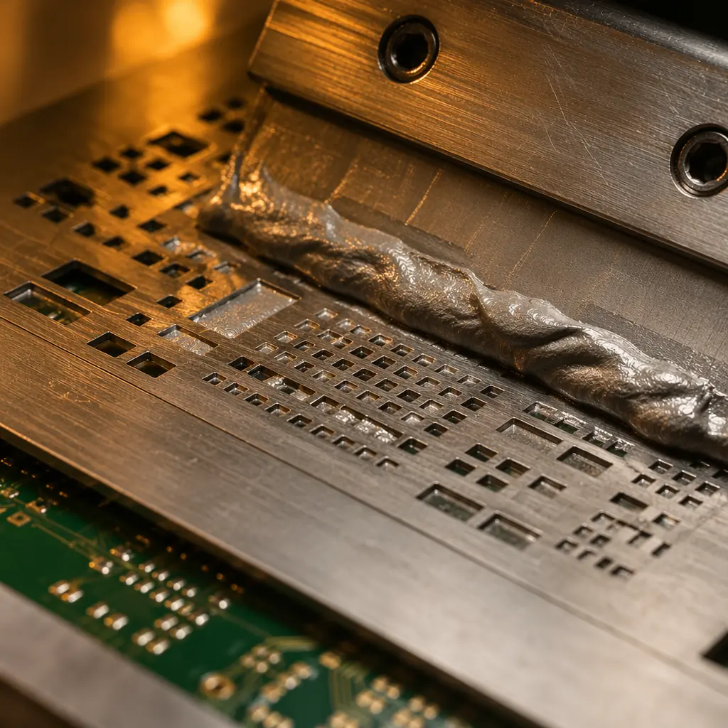
Every SMT assembly starts with precision solder paste deposition. We use laser-cut stainless steel stencils (0.08–0.20mm thickness) on DEK Horizon 03iX printers with automatic optical alignment. The printer achieves ±12.5µm alignment at 2 Cpk, critical for fine-pitch pads.
Process Step 2-3
After paste deposition and SPI verification, boards enter the placement and reflow sequence. High-speed placers (Yamaha YSM40R, 200K CPH) handle chip components while fine-pitch placers (Yamaha YSM20WR) handle BGAs and QFNs in the same pass. The entire line is synchronized for continuous flow.
Laser-cut stencil, auto-alignment. 3D SPI on every board. ±12.5µm @ 2 Cpk.
High-speed + fine-pitch placers in sequence. Vision alignment. 200K CPH.
10-zone N₂ atmosphere. Custom profile per design. ±1.5°C zone control.
Automated optical inspection on 100% of boards. AI defect classification. SPC data.
BGA/QFN X-ray inspection. Void analysis. Final visual inspection before release.
| Parameter | Standard Capability | Extended Capability |
|---|---|---|
| SMT Lines | 8 high-speed lines | Dedicated NPI line for prototypes & NPI |
| Placement Speed | Up to 200,000 CPH / line | Dual-lane concurrent placement |
| Smallest Passive | 0201 (0.6×0.3mm) | 01005 (0.4×0.2mm) |
| Largest Component | 55×55mm BGA | Larger on request |
| Fine-Pitch BGA | 0.25mm pitch minimum | |
| Fine-Pitch QFP/QFN | 0.3mm pitch minimum | |
| Placement Accuracy | ±15µm @ 3σ (fine-pitch placer) | |
| Board Size (Standard) | 50×50 – 510×460mm | Up to 1,200×510mm (extended rail) |
| Board Thickness | 0.8 – 3.2mm | 0.3 – 6.0mm |
| Stencil Thickness | 0.10 – 0.15mm | 0.08 – 0.20mm, stepped stencils |
| Solder Alloy | SAC305 (Pb-free), Sn63Pb37 (leaded) | |
| Reflow Zones | 10-zone, N₂ atmosphere, ±1.5°C per zone | |
| SPI | 3D volumetric, 100% coverage, ±1µm height resolution | |
| AOI | 3D AOI, 4-angle, 25µm resolution, AI classification | |
| Workmanship | IPC-A-610 Class 2 | IPC-A-610 Class 3 / J-STD-001 |
Upload your BOM, Gerber files, and assembly drawing. Our engineering team will return a complete DFM review, component availability, footprint validation, and stencil recommendations, within 24 hours.
Upload Gerber + BOM, 24h quote with free DFM review.