
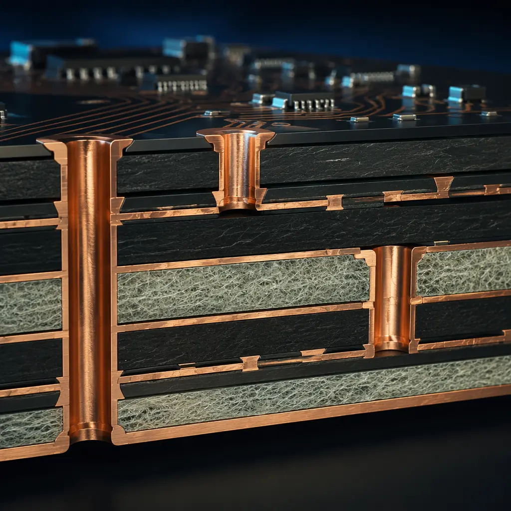
PCB Fabrication / Back Drilling
Controlled-depth drilling removes unused via stubs that cause signal reflections and degrade eye diagrams at data rates above 5 Gbps. Essential for 5G infrastructure, 100G/400G data center, and high-speed FPGA designs. Depth tolerance 50 m, X-ray verified on every board.
The Via Stub Problem
In a multilayer PCB, a plated through-hole (PTH) via extends through the entire board stack. If a signal only travels between layers 1 and 3 of a 16-layer board, the via segment from layer 3 to layer 16 is an unused "stub." At data rates above 5 Gbps, this stub acts as an unterminated transmission-line branch, causing signal reflections, resonant nulls at quarter-wavelength frequencies, and degraded eye diagrams. Back drilling removes this stub by drilling out the unused portion of the via barrel from the opposite side, leaving only the electrically necessary length.
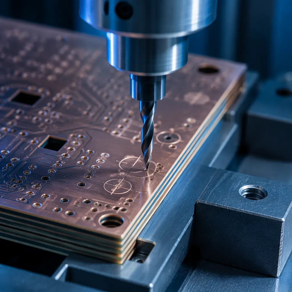
Technical Specifications
| Parameter | Specification |
|---|---|
| Drill Type | Mechanical CNC, controlled depth with precision depth collar |
| Back Drill Diameter | Original hole diameter + 0.15mm to 0.30mm oversize |
| Depth Tolerance | ±50µm (standard), ±75µm for cost-optimized designs |
| Remaining Stub Length | 50-150µm typical; shorter stubs require tighter process control |
| Layer Range | 8-32 layers (back drilling requires sufficient stack thickness) |
| Via Types Supported | PTH, blind vias, stacked microvias on through-hole back-drilled locations |
| Post-Drill Inspection | 100% X-ray verification; cross-section on first article |
| Data Format | Separate back-drill file specifying drill layers, diameters, and depths |
| Finish After Drill | Standard ENIG/HASL/OSP; back-drilled holes receive same finish as PTH |
| Burr Control | Dedicated entry/exit material; burr height <25µm post-process |
Applications
Any design with high-speed serial links running through multiple PCB layers can benefit from back drilling. The performance gain becomes critical above 10 Gbps per lane, where even a short via stub can create a resonant notch within the signal bandwidth. Modern SerDes standards demand back drilling as a standard design practice.
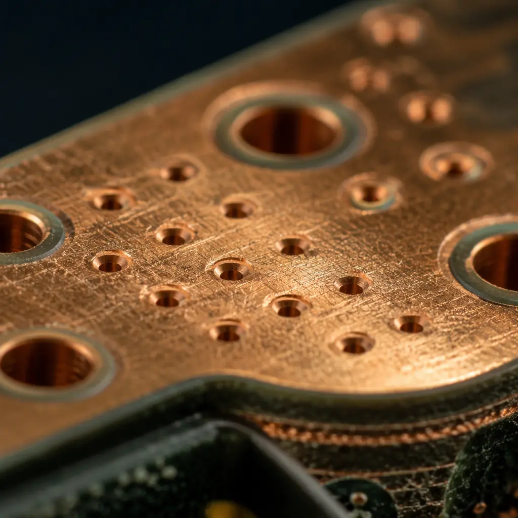
| Inspection Stage | Method | Coverage | What We Check |
|---|---|---|---|
| Depth Verification | X-Ray imaging | 100% of back-drilled holes | Stub length within tolerance; no under-drill (stub too long) or over-drill (damaged signal layer) |
| Diameter Check | AOI + mechanical pin gauge | 100% AOI; sample pin gauge | Back drill diameter matches spec; hole roundness within IPC limits |
| Cross-Section | Microsection analysis | First article; 1 coupon per panel | Stub length measured optically; copper barrel integrity; no resin smear or delamination |
| Electrical Test | Flying probe or fixture | 100% | No opens or shorts on back-drilled nets; via resistance within spec |
| Burr Inspection | Visual + microscope | 100% visual; sample microscope | Burr height under 25 m; no lifted pads at back-drill entry side |
Send us your stackup diagram and high-speed net list. Our engineering team will identify which vias need back drilling, calculate optimal drill depths, and provide a complete DFM report before production. Free back-drill feasibility review on every project.
Upload Gerber + BOM, 24h quote with free DFM review.