
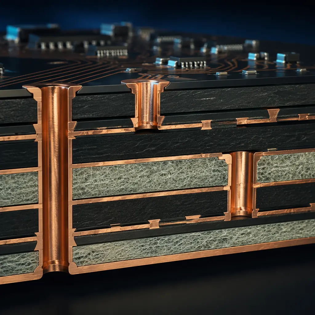
Advanced PCB / Via-in-Pad
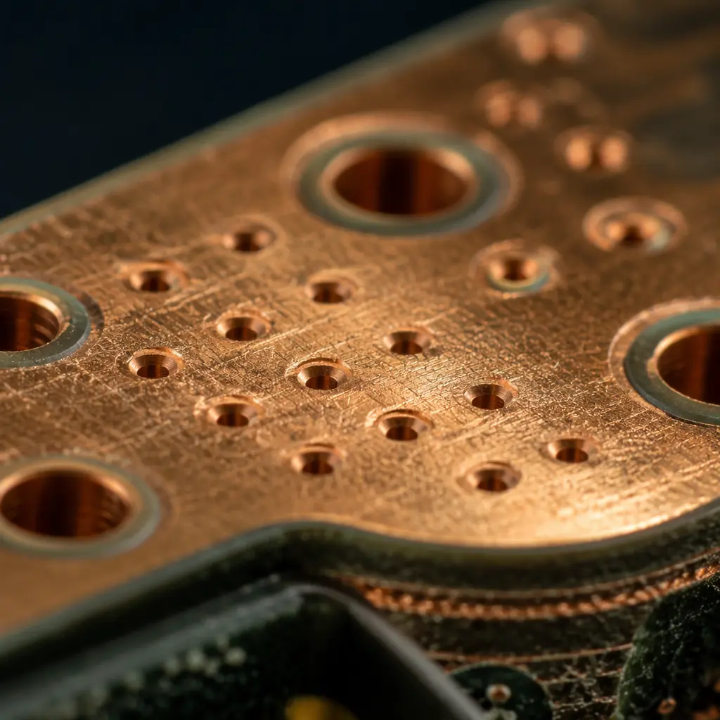
Place vias directly in SMD pads, filled with conductive or non-conductive epoxy, planarized flat, and plated over to create a perfectly solderable surface. Essential for 0.5mm-pitch BGA breakouts and high-density interconnect where every millimeter of routing space counts. IPC Class 3 qualified with 100% flatness verification.
The Density Problem
Traditional PCB routing requires a via, a trace, and a solder pad, three separate features consuming board real estate. On a 0.5mm-pitch BGA with 1,000+ balls, the breakout consumes every available layer and still constrains routing. Via-in-pad eliminates the third feature entirely: the via is placed inside the solder pad, filled with epoxy, planarized flat, and plated over. The pad surface becomes indistinguishable from a standard SMD pad, solderable, flat, and fully compatible with automated SMT assembly.

Fill Material Options
| Parameter | Non-Conductive Fill (NCF) | Conductive Fill (Cu/Ag) |
|---|---|---|
| Fill Material | Epoxy resin with inorganic filler | Silver- or copper-filled epoxy |
| Primary Use | Signal vias in pads, standard for BGA breakout | Thermal vias, heat dissipation from power devices |
| Thermal Conductivity | ~0.5 W/m·K | ~3-8 W/m·K |
| Electrical Conductivity | Insulating (prevent shorts) | Conductive (enhances thermal path) |
| CTE Match | Close to FR-4 laminate (~50 ppm/K) | Close to copper (~35 ppm/K) |
| Via Diameter Range | 0.15 – 0.50mm | 0.20 – 0.60mm |
| Copper Cap | Electroplated 15-25µm over fill | Electroplated 20-30µm over fill |
| Surface Finish | ENIG / OSP / ENEPIG over cap | Same finish as surrounding pads |
| Void Criteria | <5% void area (IPC-6012 Class 3) | <10% void area; no interconnected voids |
| Cost Impact | Standard upcharge | Moderate premium over NCF |
Process & Applications
Via-in-pad adds four steps to the standard PCB fabrication flow: drill the via, fill with epoxy (vacuum-assisted to eliminate voids), planarize the surface (mechanical scrubbing or fly-cut to remove excess fill), and electroplate a copper cap over the filled via. The result is a pad surface that is indistinguishable from a standard SMD land, flat to within 5 µm, fully solderable, and compatible with all standard surface finishes.
| Parameter | Standard | Extended |
|---|---|---|
| Min Via Diameter | 0.20mm | 0.15mm |
| Max Aspect Ratio | 8:1 (microvia); 10:1 (through via) | |
| Fill Type | Non-conductive epoxy | Conductive (Ag/Cu) epoxy |
| Flatness (Post-Planarization) | <5 µm deviation | |
| Cu Cap Thickness | 15-20 µm | 20-30 µm |
| Void Content (IPC-6012) | <5% void area per via (Class 3) | |
| Inspection Method | X-ray + cross-section on first article; 100% AOI | |
| Surface Finishes | ENIG, ENEPIG, OSP, Immersion Silver, Immersion Tin | |
| Board Thickness | 0.4-2.0mm | 0.2-3.2mm |
| Certification | IPC-A-600 Class 2 / IPC-6012 Class 3 | |
Send us your BGA placement, layer stackup, and netlist. We'll map out the via-in-pad strategy, which vias get filled, which get conductive epoxy, and how to minimize your layer count. Free via-in-pad feasibility review with every DFM check.

Upload Gerber + BOM, 24h quote with free DFM review.