
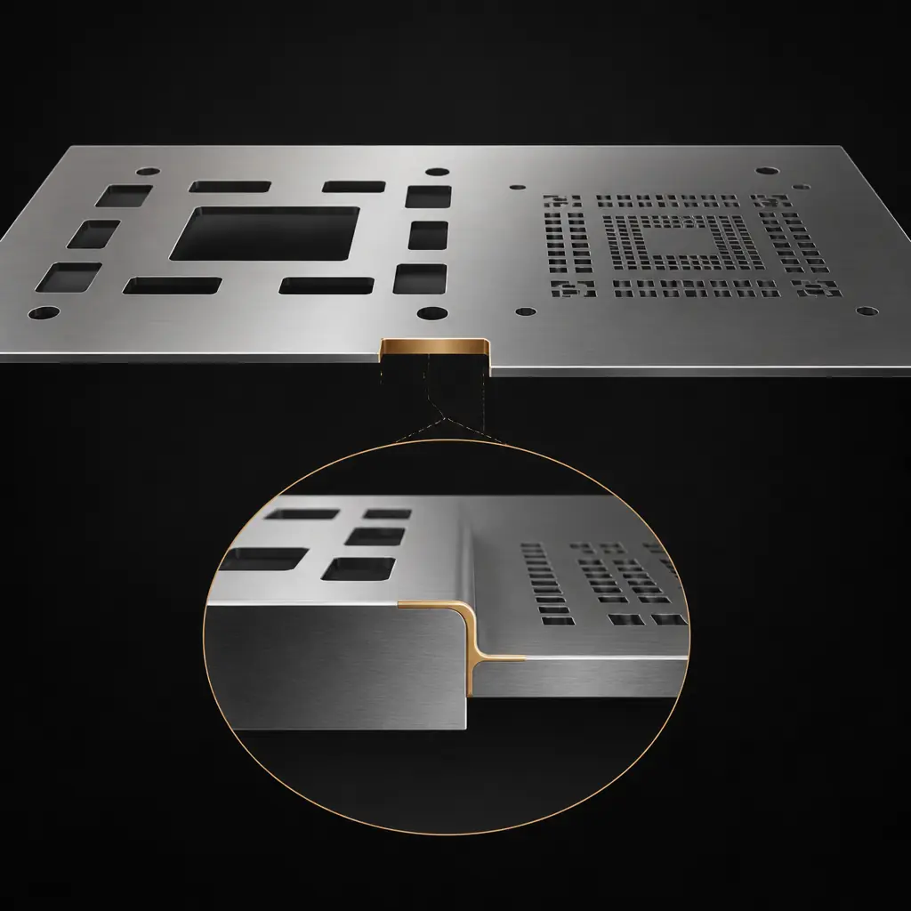
Advanced Stencil Technology
Different paste volumes for different components, on the same board, in a single print stroke. Solve the fine-pitch vs. power-component paste volume conflict with precision-engineered step stencils.
Standard stencils have uniform thickness across the entire foil. For a board carrying only 0.5mm-pitch QFNs, a 0.10mm stencil delivers ideal paste volume. But add large power MOSFETs or through-hole connectors requiring intrusive reflow solder paste on the same board, and that 0.10mm thickness starves them of solder, leading to insufficient fillets, weak joints, and field failures.
A thicker stencil (0.15mm+) solves the power-component problem but deposits too much paste on fine-pitch pads, causing bridging, solder balls, and shorts on QFNs and 0201 passives. Step stencils eliminate this trade-off by manufacturing different thickness zones in a single stencil foil, each optimized for the component mix in that area.
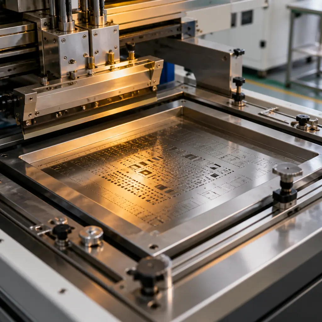
The most common configuration. The stencil starts at a thicker base (e.g., 0.15mm) and is locally etched thinner (e.g., 0.10mm) in the fine-pitch zones on the squeegee side.
The reverse approach. A thinner base stencil (e.g., 0.10mm) has material added locally (e.g., 0.18mm) for power-component zones on the board-contact side. More complex to manufacture but protects fine-pitch print quality.
Boards with DSP/MCU fine-pitch logic alongside large IGBT modules, MOSFET arrays, and high-current bus bar pads. Step-down stencil delivers 0.10mm on the logic side, 0.18mm on power devices, in one print stroke.
Modern ECUs pack 0201 decoupling caps, 0.4mm-pitch BGAs, and large connector footprints on one board. A well-designed step stencil prevents bridging on the processor while ensuring sufficient paste for high-reliability connector solder joints.
Compact wireless modules with fine-pitch RF shields and chip antennas alongside power-management ICs with exposed thermal pads. Step stencil lets you optimize paste for both without compromising RF grounding or thermal performance.
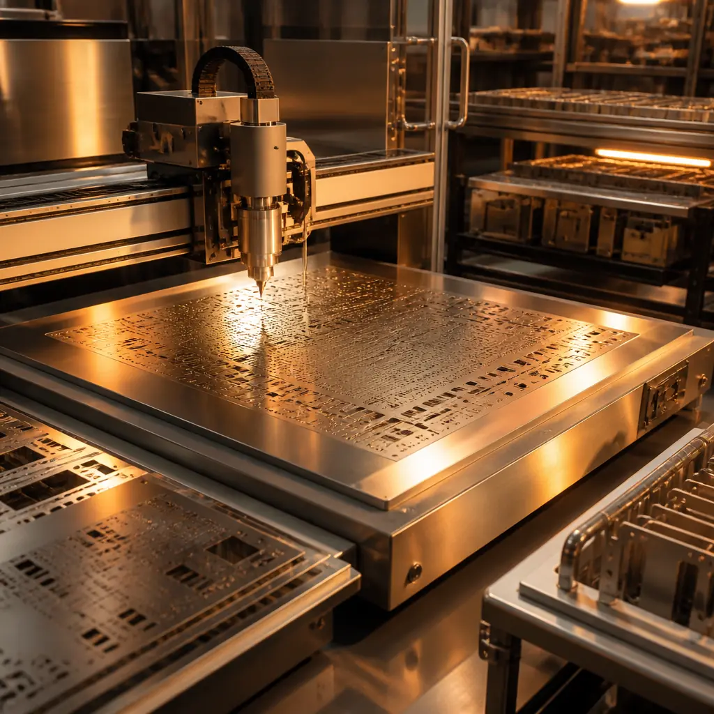
Effective step stencil design requires planning at the PCB layout stage. Keep-out zones of 2–3mm around step transitions ensure the squeegee blade rides smoothly and the stencil gaskets properly against the board surface. We recommend grouping fine-pitch components together in one contiguous zone and power/high-volume paste components in another.
The step transition itself is a gradual ramp (approximately 1mm per 0.02mm step height), not an abrupt wall. Our CAM engineers review your step plan during the DFM stage and may recommend zone adjustments to avoid aperture-distortion risk near transition areas. Multi-level stencils (3+ thickness levels) are possible but add complexity; we typically recommend a maximum of two step levels for reliable print performance.
Step-down (pocket on squeegee side) and step-up (raised on board-contact side). Two-level standard, three-level on request. Step height from 0.02mm to 0.10mm differential.
Base foil 0.08–0.15mm. Stepped zones 0.10–0.20mm. Total differential up to 0.10mm. Combination example: 0.10mm base + 0.08mm step-down = 0.18mm / 0.10mm zones.
Step-down: ≥ 2mm from step edge to nearest aperture. Step-up: ≥ 3mm clearance. Transition ramp: approximately 1mm per 0.02mm step. Detailed zone map reviewed during DFM.
Compatible with all major automatic printers (DEK Horizon/Eclipse, MPM Momentum/Accela, Ekra, GKG, Desen). Step stencils are framed only, frameless step stencils are not recommended.
304 stainless steel foil, mesh-mounted on precision aluminum frame. Nano-coating available on step stencils, recommended for fine-pitch zones to maintain release performance.
Free step-zone DFM review included. Standard turnaround: 48 hours from approved step plan. Rush: 36 hours. Complex 3+ level designs: 72 hours. Contact us for same-day feasibility assessment.
Send us your Gerber file and component placement. Our CAM engineers will propose an optimized step stencil configuration, free, no obligation.
Upload Gerber + BOM, 24h quote with free DFM review.