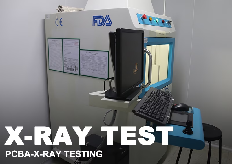
Behind every reliable automotive control unit, medical implant, or satellite circuit board lies an invisible quality guardian: PCBA-X-Ray testing. This non-destructive inspection method peers through materials to reveal hidden soldering defects that optical systems can’t detect. In an industry where a single voided BGA joint can cost millions in recalls, X-ray testing ensures microscopic perfection. Let’s explore how this technology safeguards modern electronics.
The Science of X-Ray Inspection in PCB Assembly
PCBA-X-Ray testing utilizes controlled radiation to create high-resolution images of internal board structures. Key technical components include:
1. X-Ray Source Specifications
- Microfocus Tubes: 5-160kV energy range with 0.5μm spot size
- Transmission Targets: Tungsten or copper anodes for material contrast
- Geometric Magnification: 2,000X+ resolution for 01005 components
2. Detection Systems
- Flat Panel Detectors: 16-bit depth capturing 5μm features
- Scintillator Layers: CsI(Tl) crystals converting X-rays to visible light
- Dynamic Ranges: 72dB for simultaneous solder/component imaging
3. Software Algorithms
- AI Void Detection: Classifies defects as small as 10μm²
- 3D Tomography: Reconstructs multi-layer boards in Z-axis
- Automated Reporting: IPC-610 compliance verification in <30 seconds
Why X-Ray Testing is Indispensable?
1. Hidden Defect Detection
X-Ray identifies critical flaws invisible to AOI/SPI:
| Defect Type | Minimum Detectable Size | Acceptability Threshold |
|---|---|---|
| BGA Void | 15μm diameter | <25% ball area (IPC-7095) |
| QFN Sidewall | 20% fillet deficiency | >50% coverage required |
| Barrel Fill | 75% through-hole | IPC Class 3 requirement |
2. Process Optimization
- Solder Paste Volume: Correlates SPI data with actual joint formation
- Component Shift: Measures 3D alignment of stacked packages
- Intermetallic Growth: Monitors Cu6Sn5 layer thickness (2-5μm ideal)
3. Compliance Assurance
- Automotive: AEC-Q100-012 for flip-chip attachments
- Medical: ISO 13485 Class III implantable devices
- Aerospace: NASA-STD-8739.4 for high-reliability soldering

The 5-Step X-Ray Testing Workflow
1. Program Setup
- Golden Sample Comparison: 0.5μm alignment to reference CAD
- Material Calibration: Adjusts for Cu vs. SnAgCu alloys
2. Image Acquisition
- 2D Imaging: 10-second scan for 300x300mm boards
- 3D CT Scan: 5-15 minute full layer analysis
3. Automated Analysis
Deep learning models evaluate:
- Void Percentage: <25% in BGA/CSP joints
- Filament Integrity: Continuous interconnects
- Foreign Objects: 50μm+ metallic/non-metallic debris
4. Defect Classification
AI-powered categorization:
- Critical (immediate rejection)
- Process-indicative (requires parameter adjustment)
- False calls (<0.1% occurrence)
5. Process Feedback
Closed-loop system adjusts:
- Stencil aperture designs
- Reflow profiles
- Component placement parameters
Technical Advantages Over Alternative Methods
1. Comprehensive Coverage
- Multi-Layer Inspection: Simultaneously examines top/bottom solder joints
- Material Penetration: Images through 5mm-thick aluminum heatsinks
2. Quantitative Analysis
- Void Measurement: ±0.5% accuracy in BGA balls
- Solder Thickness: 1μm resolution across 100mm² areas
3. Speed & Scalability
- Throughput: 400+ BGAs/minute on 600mm boards
- Multi-PCB Fixturing: 4-up panel inspection in single scan
Industry-Specific Applications
Automotive Electronics
- ADAS Controllers: 0-defect BGA joints for ASIL-D compliance
- EV Power Modules: Verifies 400A current paths in IGBT stacks
Medical Devices
- Implantable PCBA: 100% void-free solder joints (ISO 13485)
- MRI Components: Non-magnetic inspection for RF shields
Aerospace Systems
- Satellite Boards: Detects tin whiskers <50μm long
- Avionics: Validates conformal coating under components

Overcoming X-Ray Testing Challenges
1. False Positive Reduction
- Material Database: 500+ alloy signatures minimize misidentification
- 3D Slice Analysis: Distinguishes real voids from leadframe shadows
2. Complex Component Handling
- Tilt Compensation: 45° angled imaging for side-view fillets
- High-Z Shielding: Tungsten collimators block scatter radiation
3. Mixed-Technology Boards
- Adaptive Energy: 80kV for through-hole, 130kV for metal-core PCBs
- Multi-Layer Registration: Aligns 12+ layers with 2μm accuracy
Future Innovations in X-Ray Testing
1. AI-Driven Predictive Quality
- Forecasts solder joint reliability over 10-year lifespan
- Correlates X-Ray data with thermal/mechanical simulations
2. Ultra-High-Speed Systems
- Rolling Scan Technology: 1m/sec conveyorized inspection
- Photon-Counting Detectors: 100X faster than conventional CCD
3. Eco-Friendly Solutions
- Low-Energy Systems: 40kV operation reduces power by 60%
- Automated Shielding: AI-optimized radiation containment
PCBA-X-Ray testing has evolved from niche inspection to essential quality assurance in electronics manufacturing. As components shrink below 01005 sizes and power densities increase, this technology remains crucial for verifying reliability where it matters most—inside the joint.
For X-Ray inspection solutions meeting IPC Class 3 and medical-grade standards, contact our engineering team at sales@huaxingpcba.com. With expertise in mission-critical assemblies, we ensure your PCBs pass the most stringent hidden defect checks.


