
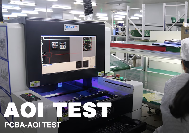
Modern smartphones contain over 12,000 solder joints on a circuit board no larger than a credit card. Ensuring every microscopic connection meets quality standards would be impossible without PCBA-AOI (Automated Optical Inspection). This technology detects defects invisible to the human eye, safeguarding everything from medical implants to satellite systems. Let’s explore how AOI maintains quality in today’s ultra-miniaturized electronics.
How AOI Technology Works in PCB Assembly
AOI systems combine advanced optics, precision mechanics, and AI-powered software to inspect PCBs at speeds exceeding 25,000 components per hour. The process involves three core components:
1. High-Resolution Imaging
- Cameras: 20-50MP global shutter cameras capture 3-5μm/pixel details
- Lighting: Multi-angle LED arrays (red/blue/white) highlight surface variations
- 3D Profilometry: Laser triangulation measures solder height within ±5μm
2. Algorithm-Driven Analysis
- Template Matching: Compares images against golden board references
- Deep Learning: Neural networks trained on 1M+ defect samples achieve 99.98% accuracy
- Defect Classification: Distinguishes tombstoning, bridging, and missing components
3. Real-Time Feedback Loop
- NG Marking: Flags defects with 0.1mm positional accuracy
- SPC Integration: Updates control charts for process optimization
The Critical Role of AOI in SMT Manufacturing
1. Defect Detection Capabilities
AOI identifies 98% of critical soldering issues:
| Defect Type | Detection Rate | Acceptability Threshold |
|---|---|---|
| Solder Bridging | 99.9% | <0.1mm gap between pads |
| Component Shift | 99.7% | >0.05mm misalignment |
| Insufficient Solder | 99.5% | <75% pad coverage |
2. Yield Improvement Metrics
- First-Pass Yield: Increases from 92% to 99.5% in high-density designs
- Rework Reduction: Cuts post-assembly repairs by 80%
- Cost Savings: $18K saved per 10K boards via early defect detection
3. Compliance Assurance
- IPC-A-610 Class 3: Validates military/aerospace standards
- ISO 9001: Documents 100% inspection traceability
AOI vs. Human Visual Inspection: A Data-Driven Comparison
| Parameter | AOI | Human Inspectors |
|---|---|---|
| Speed | 0.5 sec/component | 2-3 sec/component |
| Accuracy | 99.95% | 85-90% |
| Consistency | 24/7 stable performance | Fatigue-induced error spikes |
| Defect Types | 50+ categorized defects | Limited to visible issues |
| False Call Rate | <0.1% (with AI) | 5-8% |
Industry-Specific Applications of AOI Testing
Automotive Electronics
- ADAS Controllers: Detects micro-cracks in 0.3mm-pitch CAN transceivers
- EV Battery Modules: Verifies 300A busbar soldering integrity
Medical Devices
- Implantable PCBA: Ensures 0 voids in hermetically sealed joints
- Surgical Robotics: Validates 0.4mm flex circuit alignments
Aerospace Systems
- Satellite Boards: Flags whisker growth in tin-based solders
- Avionics: Certifies conformal coating uniformity (MIL-I-46058C)
Overcoming Common AOI Implementation Challenges
1. False Positives Reduction
- Multi-Algorithm Voting: Combines rule-based and AI models
- 3D Height Thresholds: Ignores harmless solder variations <20μm
2. Complex Programming
- Auto-Learning Systems: Koh Young KY8030 requires 30% less setup time
- Component Libraries: Pre-loaded 50K+ device profiles (IPC-7351B compliant)
3. Mixed-Technology Boards
- Hybrid Algorithms: Simultaneously inspects 01005 chips and through-hole connectors
- Dynamic Lighting: Adjusts angles for reflective vs. matte surfaces
Future Trends in Automated Optical Inspection
1. AI-Driven Adaptive Systems
- Self-Optimizing Algorithms: Reduce programming time from hours to minutes
- Predictive Quality: Forecasts defects 10 process steps ahead
2. 3D+2D Hybrid Inspection
- Co-Planarity Checks: Measures component tilt within 0.5°
- Hidden Joint Analysis: Laser-scans QFN sidewall fillets
3. Integrated Process Control
- SPI-AOI-X-Ray Feedback Loop: Closes 95% of process variation sources
- Digital Twin Integration: Simulates inspection results pre-production
PCBA-AOI testing has evolved from simple pass/fail checks to a sophisticated quality assurance ecosystem. As component sizes approach 01005 (0.4×0.2mm) and lead-free alloys demand tighter process windows, AOI remains the guardian of reliability in electronics manufacturing.
For AOI solutions meeting IPC Class 3 and medical-grade standards, contact our engineering team at sales@huaxingpcba.com. With 15+ years of expertise, we optimize inspection processes to achieve <10 ppm defect rates in mission-critical assemblies.


