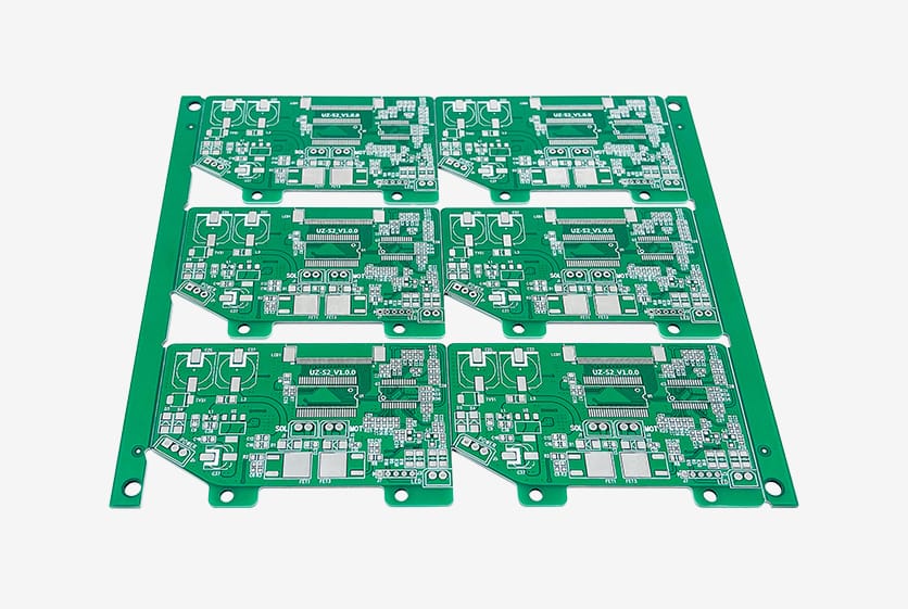
Printed Circuit Boards (PCBs) are the foundation of modern electronics, and their layers play a critical role in determining their functionality, complexity, and performance. From single-layer designs to advanced multi-layer systems, the evolution of PCB layers has been driven by the need for higher density, better signal integrity, and improved thermal management. This article explores the design and production of PCB layers, their development over time, and their impact on the electronics industry.

Single-Layer PCBs: The Starting Point
Design and Production:
Single-layer PCBs, introduced in the 1950s, consist of a single conductive layer of copper laminated onto an insulating substrate, typically phenolic resin or paper. The design process involves etching the copper layer to create conductive pathways, while components are mounted on one side. Production is straightforward, involving printing, etching, and drilling.
Applications:
Single-layer PCBs are cost-effective and ideal for simple devices like radios, calculators, and basic consumer electronics.

Double-Layer PCBs: A Step Forward
Design and Production:
Double-layer PCBs, developed in the 1960s, feature conductive layers on both sides of the substrate. The key innovation was the introduction of plated-through holes by Motorola in 1953, which allowed electrical connections between the two layers. Designers could now route more complex circuits, and production involved additional steps like hole plating and double-sided etching.
Applications:
Double-layer PCBs enabled the development of early computers, telecommunications equipment, and more advanced consumer electronics.

Multi-Layer PCBs: Complexity and Performance
Design and Production:
Multi-layer PCBs, pioneered in the 1970s, stack multiple conductive layers separated by insulating materials. The design process requires careful planning of signal integrity, power distribution, and thermal management. Production involves laminating layers together, drilling vias, and plating through-holes to connect the layers. Litton Systems introduced the first 6-layer PCB in 1960, and the use of FR-4 (fiberglass-reinforced epoxy) became standard for its durability and thermal properties.
Applications:
Multi-layer PCBs are used in complex systems like mainframe computers, aerospace equipment, and medical devices, where high circuit density and reliability are essential.

HDI PCBs: Pushing the Limits
Design and Production:
High-Density Interconnect (HDI) PCBs, developed in the 1990s, utilize microvias, finer traces, and multiple layers of interconnects to achieve even greater component density. Panasonic’s ALIVH (Any Layer Interstitial Via Hole) technology, introduced in 1995, was a major breakthrough. HDI PCB design requires advanced software to manage the intricate routing, while production involves laser drilling and precise layer alignment.
Applications:
HDI PCBs are essential for modern electronics like smartphones, tablets, and wearable devices, where space and performance are critical.
Performance Comparison of PCB Layers
The table below summarizes the key characteristics of different PCB layers:
| PCB Type | Layer Count | Key Features | Applications |
|---|---|---|---|
| Single-Layer | 1 | Simple design, low cost | Radios, basic electronics |
| Double-Layer | 2 | Plated-through holes, higher density | Early computers, telecom equipment |
| Multi-Layer | 4-12 | Enhanced signal integrity, compact design | Mainframes, aerospace systems |
| HDI Multi-Layer | 16+ | Microvias, fine traces, high density | Smartphones, servers, medical devices |
FAQs
1. What are the main types of PCB layers?
The main types are single-layer, double-layer, multi-layer, and HDI (High-Density Interconnect) PCBs.
2. How are multi-layer PCBs produced?
Multi-layer PCBs are produced by laminating multiple conductive layers with insulating materials, drilling vias, and plating through-holes to connect the layers.
3. What is the role of vias in PCB design?
Vias are used to create electrical connections between different layers of a PCB, enabling complex circuit routing.
4. What are the advantages of HDI PCBs?
HDI PCBs offer higher component density, better signal integrity, and reduced size, making them ideal for compact, high-performance devices.
5. What materials are commonly used in PCB production?
Common materials include FR-4 (fiberglass-reinforced epoxy), polyimide, and ceramic substrates, depending on the application’s requirements.


